This invention provides a method for fabricating a silicon-based device that integrates high-temperature processed PCMO-RRAM with a Si-PN junction-based selector. The approach addresses the compatibility challenges associated with integrating materials that require high-temperature annealing in reactive environments. The work compared different integration strategies and the electrode-last approach is the suitable one for the high temperature processed RRAM devices. This enables the reliable construction of selector-memristor integrated bit-cells suitable for memristor crossbar arrays, paving the way for energy-efficient, high-throughput, in-memory computing systems.

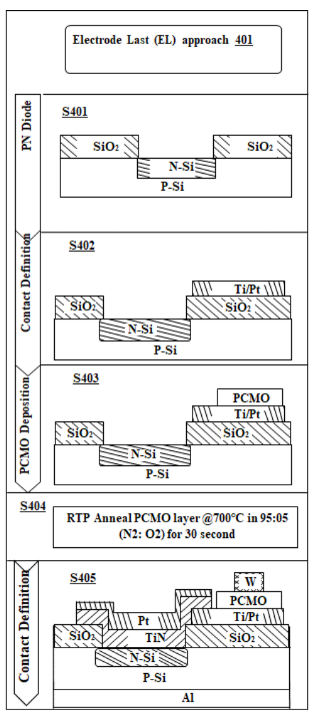
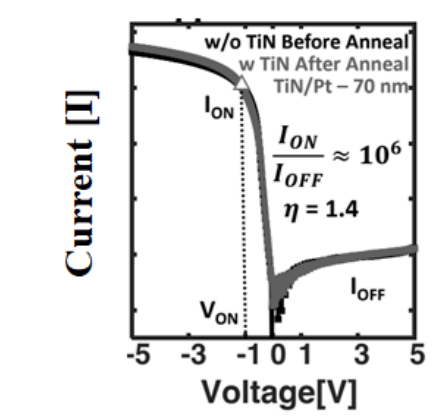
Figure (1) Flow diagram illustrating a method of integrating the high-temperature processed RRAM with the Si-PN junction-based selector for the silicon devices using the electrode last approach; (2) Diagram illustrating integration of the high temperature processed RRAM with the Si-PN junction based selector for the silicon devices using an electrode last approach; (3) Si-PN junction V-I characteristics of the integrated bit cell of the silicon device before and after high-temperature PCMO annealing for the electrode last approach.
Recent advances in PCMO-based Resistive Random Access Memory (RRAM) devices show promise for analog memory and in-memory computing due to their non-volatility, low variability, and scalability. However, integrating high-temperature processed PCMO-RRAM with silicon (Si)-based selector devices such as Si-PN junctions remains challenging. The key difficulty lies in preserving the Si-junction characteristics and metal interconnect stability during the high-temperature annealing process required for PCMO crystallisation, which may degrade Si junctions or interconnects and affect device performance. A robust, process-compatible method for integrating these devices on the same substrate is therefore necessary.
- Monolithic Integration of Selector and Memory: This technology enables the seamless integration of PCMO-based RRAM with silicon-based selectors (such as PN junctions, NPN, NIPIN, and MOSFETs) on a single substrate.
- Thermal Compatibility through Electrode Engineering: It allows high-temperature annealing (up to 700°C) without degrading silicon junctions or interconnects, using carefully engineered electrode stacks and diffusion barriers.
- Versatile Integration Schemes: This innovation compares different approaches to find the one which actually works:
• Electrode-last approach – where metal interconnects are formed after annealing
• Common electrode approach – using a shared metal layer before annealing
• Separate electrode approach – involving overlapping distinct metals before annealing
- Foundry-Compatible Process Flow: This technology is compatible with standard semiconductor fabrication processes, making it suitable for integration into existing foundry workflows.
The prototype consists of a silicon substrate with thermally grown silicon dioxide (SiO2) and a precisely defined Si-PN junction. The PCMO resistive switching material is deposited using radio frequency (RF) sputtering and subsequently annealed at 700°C in a controlled nitrogen-oxygen (N2:O2) atmosphere to activate its properties. Electrical interconnections are formed using titanium/platinum (Ti/Pt) bilayers along with titanium nitride (TiN) diffusion barriers to protect sensitive regions. The top electrode, typically tungsten (W), is deposited after the annealing process, while aluminium (Al) is thermally evaporated to form the P-metal contact.
Integration with PN junctions is completed. Ongoing exploration with NPN, NIPIN-based silicon devices.
4
This technology enables next-generation computing platforms that offer higher energy efficiency and improved performance, particularly benefiting AI and machine learning workloads. It helps reduce the memory-compute bottlenecks commonly faced in large-scale data processing tasks. Additionally, it supports the development of scalable, low-power electronic devices essential for edge computing and embedded systems. Furthermore, the technology advances indigenous microelectronics research and development capabilities.
- In-memory computing
- Neuromorphic hardware
- Semiconductor foundries and IC fabrication
- Edge AI and IoT devices
- Advanced computing architectures and accelerators
- Data centres and high-performance computing (HPC)
Geography of IP
Type of IP
202321013267
564315