The invention relates to an electronic device and method for training on-chip artificial neural networks (ANNs) using in-memory computing (IMC). It overcomes the inefficiencies of traditional von Neumann architectures by integrating memory and computation directly, minimising data movement and enabling energy-efficient, low-latency, on-chip training.
The device comprises a neural network management controller that includes neurons and transposable memory elements, which cooperatively store and update activation, error, and weight parameters. This enables highly parallelised and scalable ANN training suitable for edge AI applications.
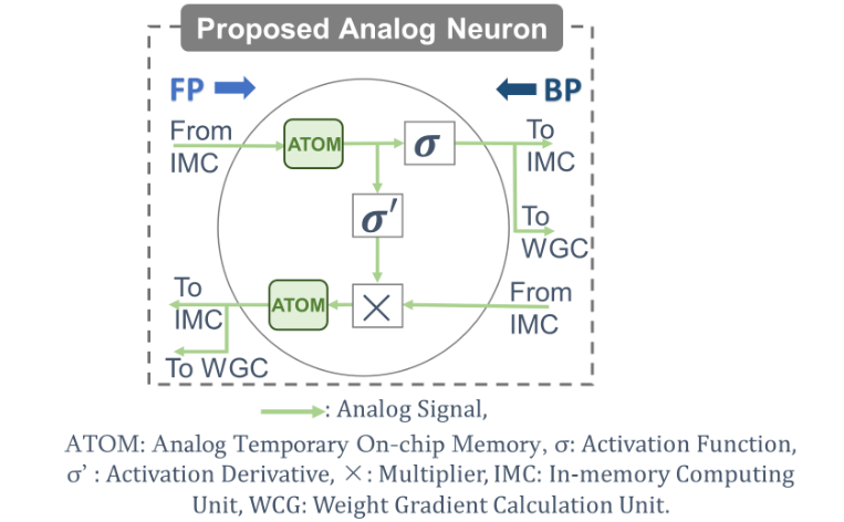


Figure (1) Proposed ANN Neuron architecture; (2) A flow chart illustrating a method for performing the training operation in an on-chip ANN; (3) The performance comparison between the baseline and the proposed system for various performance parameters
The training of Artificial Neural Networks (ANNs) typically relies on digital von Neumann architectures, which separate memory and computation, leading to the "Memory Wall" bottleneck-where energy and time are mostly spent moving data rather than computing. This becomes especially inefficient during training, which involves frequent, large-scale data transfers.
While GPUs and TPUs accelerate training via parallelism, they are impractical for edge environments due to their size, power demands, and reliance on centralised infrastructure. As AI increasingly moves to the edge (e.g., IoT, wearables, autonomous systems), there is a pressing need for compact, energy-efficient training solutions that can function within limited hardware resources.
- On-Chip ANN Management: The invention provides an ANN controller embedded within the chip that performs training directly, without requiring external computational support.
- In-Memory Computing Architecture: The technology implements in-memory computing (IMC), which performs computations at the memory location itself. This eliminates the constant data shuffling between memory and processor, significantly reducing latency, energy usage, and training time-especially crucial for edge AI devices.
- Dual-Path Neuron Design for Forward and Backward Propagation: Each neuron uses two separate memory units – one for storing activation parameters and one for error parameters – enabling simultaneous and efficient execution of both forward and backward passes necessary for training neural networks.
- Transposable Memory Devices: These allow for real-time updating of weights during training using locally stored activation and error values, minimizing the need for off-chip resources.
- Real-Time Learning & Overwriting: Memory units (first, second, third) are dynamically overwritten with new values as new inputs are processed, enabling continuous and real-time learning.
The prototype is an integrated electronic device designed to train ANNs on-chip using a memory-centric architecture. It features an ANN management controller made up of a network of neurons, each coupled with transposable memory units. These neurons perform local processing: during the forward pass, they generate activation parameters, and during the backward pass, they generate error signals.
A training manager associated with each transposable memory unit uses these values to compute and update weight parameters stored locally. The device includes input and target management units, which provide input signals and target datasets for real-time learning. Notably, all activation, error, and weight update parameters are stored and updated within dedicated memory blocks, ensuring minimal off-chip communication. This modular, efficient system enables low-latency, low-power ANN training, ideal for embedded and edge AI applications.
This invention is in its stage of testing and evaluation stage for the final objective.
3
This invention enables real-time learning at the edge – in devices like mobile phones, wearables, and IoT sensors – making AI more accessible, adaptive, and energy-efficient. This modular, efficient system enables low-latency, low-power ANN training, ideal for embedded and edge AI applications. It reduces dependence on cloud computing, promoting privacy-preserving, low-latency, and autonomous AI solutions for sectors like rural healthcare, smart agriculture, and real-time industrial monitoring.
- Edge AI Devices: Smartphones, IoT, wearables
- Healthcare: On-device patient monitoring & diagnostics
- Autonomous Vehicles: Real-time decision making
- Consumer Electronics: Voice and image recognition
- Defence & Aerospace: On-board learning in remote environments
Geography of IP
Type of IP
202221001342
553111