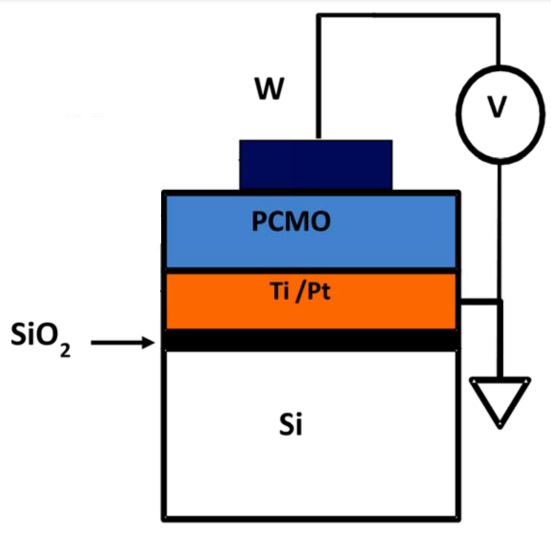
This invention addresses the complexity and cost issues in existing RRAM technologies by introducing a selector-less RRAM with integrated non-linearity within a single memory layer. The innovative design achieves high non-linearity (100-10000x) and a sharp slope (10-100 mV/dec) in the low resistance state (LRS) without the need for additional non-linear devices or layers. Utilizing a perovskite oxide layer (ABO3-δ) and combining noble and reactive metals, this solution simplifies fabrication, reduces operating voltages and costs, and enhances device performance. Relevant to semiconductor manufacturing, memory device production, and electronics, this technology offers advantages in non-volatile memory applications and high-density storage, contributing to more efficient and cost-effective memory devices.
Existing Resistance Random Access Memory (RRAM) technologies require additional non-linear devices (selectors) such as transistors or diodes, which increase operating voltages, process complexity, and fabrication costs. This invention addresses the problem by developing a selector-less RRAM with integrated non-linearity within a single memory layer, eliminating the need for additional layers or devices.
- Integration of non-linearity within a single memory layer – simplified fabrication process by eliminating the need for additional non-linear devices or layers
- High non-linearity in the range of 100-10000x
- Sharp slope in LRS in the range of 10-100 mV/dec – enhanced device performance with high non-linearity and sharp slope in LRS
- Large memory window in the range of 10-1000x – better data retention and reliability
- Use of a perovskite oxide layer (ABO3-δ) for resistance switching
- Reduced operating voltages and costs
The prototype comprises a semiconductor substrate with a first metal layer (noble metal like Pt, Au, Ru) deposited using an adhesion layer (Ti), followed by an oxide layer (complex perovskite structure ABO3-δ), and a second metal layer (reactive metal like Al, Ti, W, TiN).
The fabrication of the selector-less RRAM device has been successfully demonstrated. Electrical characterization of these devices has been completed for synapse and neuron implementation in memory and neuromorphic computing applications. The ongoing efforts focus on integrating these devices at the network level with other peripheral networks for real-time embedded applications.
6
This technology can lead to more efficient and cost-effective memory devices, contributing to advancements in consumer electronics, data storage solutions, and computing technologies, ultimately benefiting end-users with improved device performance and reliability.
- Memory device production: Non-volatile memory devices, High-density memory storage
- Electronics and computing: Consumer electronics, Industrial computing systems. Mobile devices
- Semiconductor manufacturing
- Data storage solutions
Geography of IP
Type of IP
3866/MUM/2015
394699

