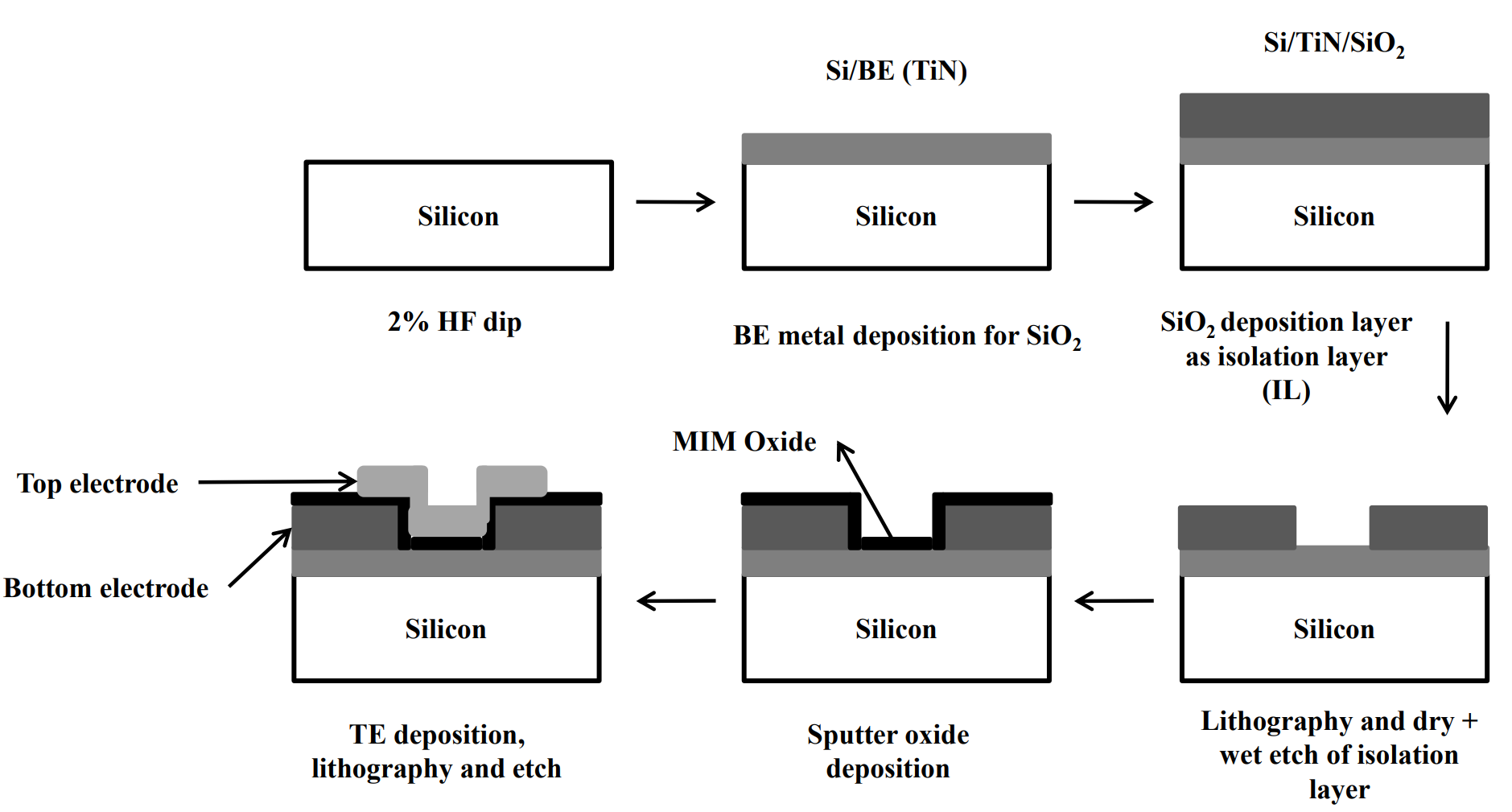
The invention provides a one-time programmable (OTP) memory device that integrates seamlessly with standard CMOS processes. It employs a Metal-Insulator-Metal (MIM) structure to create a reliable and secure memory that can generate security keys through a deterministic or probabilistic breakdown procedure. This approach eliminates the need for additional masks and process modifications while ensuring high security and reliability.
Current embedded memory solutions require additional masks and process modifications to standard CMOS flows, making them incompatible and less efficient. The need for secure, reliable, and CMOS-compatible memory for various applications such as chip IDs, analog trimming, and code storage remains unmet. Existing methods, including gate oxide breakdown and other anti-fuse technologies, do not fully address these needs due to limitations in security, compatibility, and operational efficiency.
- MIM Structure: This technology utilizes a Metal-Insulator-Metal layer configuration for the memory device.
- Breakdown Procedure: It generates security keys based on the electrical breakdown of the MIM structure, which can operate in deterministic or probabilistic modes.
- High Security: It is enhanced by the randomness in the MIM breakdown process.
- Reliability: It is robust against cloning and duplication attempts.
- Flexibility: It can operate in deterministic or probabilistic modes to generate keys
- CMOS Compatibility: It is designed to integrate with standard CMOS processes without additional masks or modifications.
- Fabrication Process: It involves depositing multiple layers (electrodes, isolation layer, MIM layer) using standard techniques like RF reactive metal deposition, dielectric sputter process, and chemical vapor deposition.
The prototype includes a substrate layer with a first electrode, an isolation layer, and a MIM layer, followed by a second electrode. The device operates by inducing an electrical breakdown in the MIM layer to generate security keys. The breakdown voltage can be controlled based on the size of the device and the desired mode of operation.
The OTP memory has been fabricated in back-end-of-line at SCL Fab in India with 180 nm CMOS Fab line. This indigenous OTPM is in stage of demonstration for security key generation for security devices like smart card.
8
The invention provides a robust, secure method for data storage and authentication, enhancing the security of electronic transactions and sensitive data. It helps protect against data breaches and unauthorized access, thereby fostering trust in electronic systems and reducing the risk of identity theft and fraud.
- Semiconductor Industry: Secure storage for secure embedded memory solutions in chips
- Analog Trimming: In precision analog circuits
- Yield Enhancement: In semiconductor manufacturing processes
- Consumer Electronics, Authentication Systems: Generation of unique security keys for secure access in devices requiring secure memory for IDs and authentication
- Chip Identification: Embedding unique IDs in semiconductor chips
- Automotive Industry: For secure, reliable storage in automotive electronics
- Financial Services: In secure transaction systems and hardware security modules
- Telecommunications: For secure storage in communication devices
Geography of IP
Type of IP
201621031483
492478

