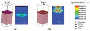
A photodiode is a device capable of converting light energy into electrical signal. The materials used to make these devices critically define the properties and performance of the photo-devices. Thus the materials primarily act as a detrimental factor in limiting the performance of these photo- devices. This bottleneck can be removed partially by using plasmonic structures which can be fabricated easily by two-photon lithography (TPL).
At the Nanostructures Engineering and MOdeling NEMO) Laboratory, we have taken a leap forward by incorporating plasmonic structures fabricated using two-photon lithography to enhance the performance of the solar cells as well as photo- detectors. We have tested the performance of these plasmonic structures on different type of solar cells. The efficiency of was found to increase by at least 20% without any optimisation for coupling, by simply placing them on the devices. In a broader perspective, this innovation is expected to revolutionise the photo-devices industry fabricating solar cells, photo detectors, microscopy, etc. by enhancing the efficiency/ improving the resolution of imaging devices.
Prof. Shobha Shukla