A new, simple way to add tiny “–OH” groups to graphene at room temperature using just hydrogen peroxide and UV light has been developed. Starting with either lab-grown or peeled-off graphene, the method cleans, coats, transfers, and treats the sheets in a straightforward sequence. Tests confirm the graphene gains useful surface features while keeping its excellent electrical performance.
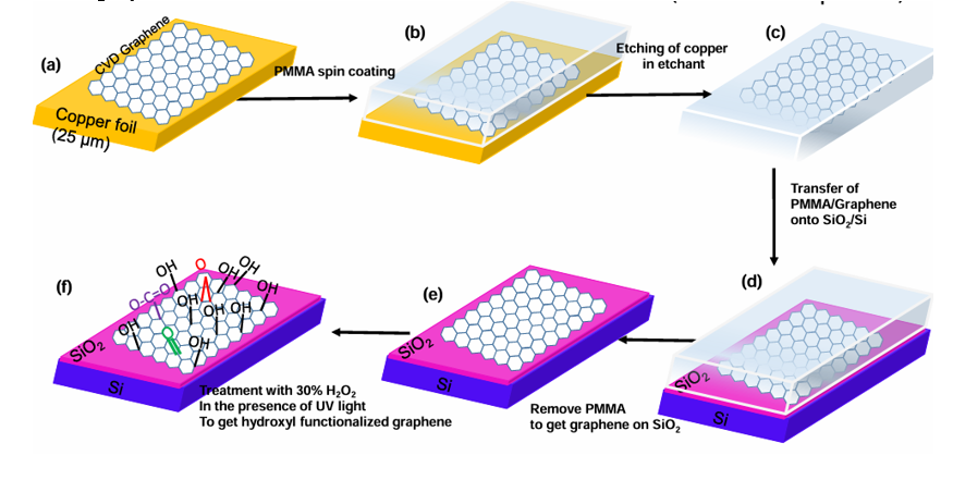
Figure 1. Schematic of the process flow for hydroxylation of CVD graphene: PMMA coating on copper foil, etching, transfer to SiO2/Si, PMMA removal, and H2O2/UV treatment.
Graphene is a powerful material with great potential in electronics and sensors, but it needs to be specially treated to work in these applications. Most existing methods to modify graphene are either expensive, produce impurities, or require high temperatures. This makes it difficult to use graphene in real-world products and industries.
- Room-Temperature Eco-Friendly Process: This technology uses only hydrogen peroxide and UV light at ambient conditions, cutting energy use and avoiding harsh chemicals.
- Pure Surface Functionalization: It evenly attaches hydroxyl groups without contaminants, ensuring a clean and reliable graphene finish.
- Electrical Performance Preservation: It maintains graphene’s superior conductivity, outperforming other modified forms like graphene oxide.
- Scalable and Simple Setup: It relies on common lab equipment (spin coater, UV lamp, etchant bath), pointing to easy scale-up for industrial production.
Lab-scale setups include a spin coater for polymer coating, a simple etching bath, and a UV lamp positioned over treated graphene on a glass or silicon wafer. Small sample sizes (0.5–1 cm2) are run through the full sequence, yielding consistent, hydroxyl-rich graphene sheets ready for testing.
The technology has been successfully demonstrated in a laboratory environment. Experiments using standard tools like Raman and XPS confirm that the graphene has been treated properly and effectively.
4
By cutting energy use and eliminating harsh chemicals, this method significantly lowers the carbon footprint and reduces toxic waste from graphene production. Making high-quality graphene more affordable unlocks advanced water-quality sensors that can detect pollutants in real time, enabling cleaner drinking water for communities. It also paves the way for longer-lasting, energy-efficient electronic devices—meaning fewer replacements and less e-waste over time. In healthcare, the availability of pure, functionalized graphene could lead to more sensitive point-of-care diagnostics, improving early disease detection. As industries adopt these greener processes, demand for skilled workers in sustainable materials processing and clean-tech manufacturing will grow, supporting new jobs and advancing broader environmental goals.
- Flexible Printed Electronics: Enables lightweight, bendable circuits for wearables and smart labels through reliable graphene inks
- High-Sensitivity Chemical and Biosensors: Offers ultra-responsive detection of gases or biomolecules thanks to its functionalized surface
- Energy Storage Devices (Supercapacitors, Batteries): Improves charge storage and cycling stability by enhancing electrode–electrolyte interactions
- Coatings for Corrosion Resistance: Forms uniform, protective graphene layers that block moisture and prevent metal degradation
- Semiconductor and Nano-Device Fabrication: Provides high-quality graphene channels for next-generation transistors and nanoscale components
Geography of IP
Type of IP
201921018594
368329