The invention provides a single-step thermal evaporation method for fabricating phase-pure organo-inorganic hybrid perovskite thin films of the formula MAPbX₃, where X represents halides such as Cl⁻, Br⁻, or I⁻. The process involves thermally evaporating pre-synthesized perovskite nanoparticles directly onto various substrates including glass, ITO, FTO, silicon, and flexible polymers. The resulting films are uniform, dense, and stable under ambient conditions, and the method eliminates the need for toxic solvents or post-deposition annealing, offering a scalable and environmentally friendly approach suitable for optoelectronic applications.
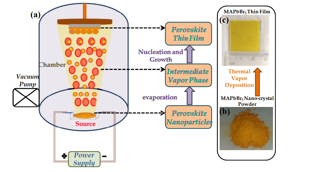
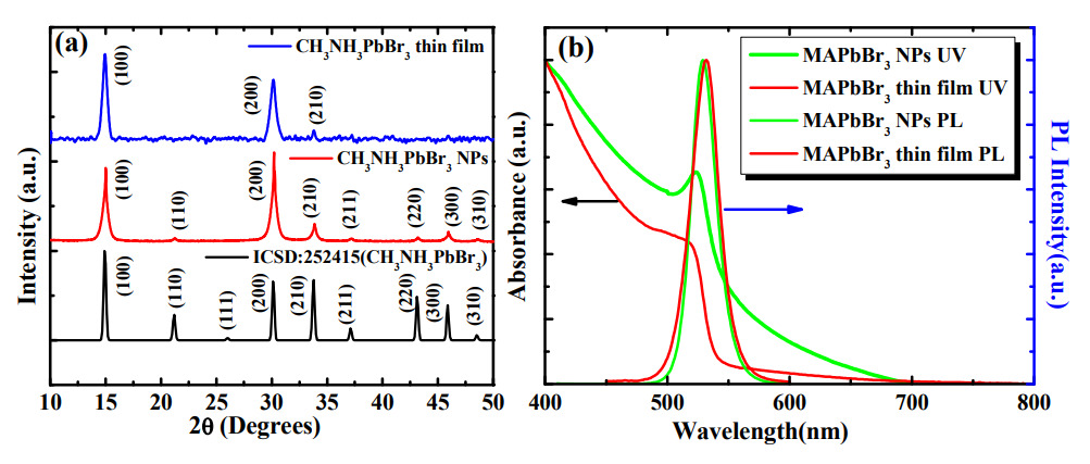
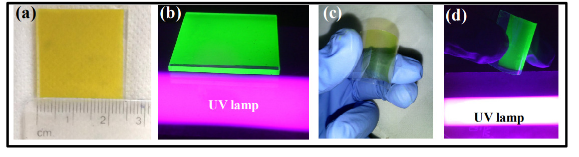
Figure (1a) Schematic diagram of single source thermal vapour deposition of MAPbX3 NPs, digital images of (1b) MAPbBr3 nanoparticle powder and (1c) as deposited MAPbBr3 thin film; (2a) XRD spectra of the MAPbBr3 thin film compared with MAPbBr3 NPs, and ICSD (252415) database of MAPbBr3, (2b) UV-vis absorption and photoluminescence (PL) spectra of MAPbBr3 NPs (green), and MAPbBr3 thin films (red); (3) MAPbBr3 thin films (3a) and (3b) on 1" × 1" glass substrate, (3c) and (3d) on flexible substrate. Fig. (3a) and (3c) show the as-deposited thin films under white light whereas fig. (3b) and (3d) show the emissive nature of the thin films under UV light.
Conventional techniques for fabricating organo-inorganic hybrid perovskite thin films, such as solution-based or multi-step vacuum deposition methods, often result in poor film uniformity, incomplete precursor conversion, and unstable material phases. These limitations are due to the use of toxic solvents, complicated processing steps, and difficulty in controlling precursor diffusion and reaction dynamics. There is a pressing need for a simple, reproducible, and solvent-free method that enables the direct formation of high-quality, phase-pure perovskite thin films on a wide range of substrates for optoelectronic applications.
- Single-Step Thermal Deposition Method: The process uses direct thermal evaporation of MAPbX₃ (where X = Cl, Br, or I) nanoparticles to form organo-inorganic perovskite thin films in a single step.
- No Solvents or Annealing Required: This method does not require toxic solvents or additional annealing steps, thereby simplifying processing and reducing environmental and safety concerns.
- High Uniformity and Stability: The deposited perovskite films demonstrate smooth surface morphology, dense packing, and long-term stability under ambient conditions.
- Flexible Substrate Compatibility: Thin films can be reliably formed on diverse substrates, including glass, silicon, ITO, FTO, and flexible polymeric materials.
- Scalable and Reproducible: Controlled parameters such as pressure, current, and deposition time ensure consistent film quality across multiple fabrication cycles.
The prototype was developed by thermally evaporating MAPbX₃ (X = Cl, Br, or I) perovskite nanoparticles onto substrates such as glass, silicon, FTO, and flexible ITO-coated PET sheets. A low-temperature resistive heating setup was used to sublimate the pre-synthesized powder under controlled vacuum (~10⁻⁶ mbar), current (10–12 A), and time (1–3 minutes). The deposited films exhibited uniform coverage, smooth morphology, and ambient stability, confirming the feasibility of the single-step solvent-free process for large-area thin film fabrication.
The fabrication process has been demonstrated successfully at the laboratory scale, with perovskite thin films deposited on various substrates including glass, silicon, ITO, and PET. The films showed uniformity, phase purity, and long-term ambient stability. The technology is currently validated through experimental trials and is ready for further scale-up and integration into optoelectronic device development.
4
This technology enables cost-effective, scalable fabrication of high-quality perovskite films without toxic solvents or energy-intensive post-processing, supporting environmentally sustainable manufacturing. Its applicability to flexible substrates facilitates the development of next-generation lightweight solar panels and optoelectronic devices, thereby promoting clean energy access and reducing the environmental footprint of conventional photovoltaic technologies.
- Photovoltaics and solar energy industry: For fabrication of efficient and stable perovskite solar cells
- Optoelectronic device fabrication: Including sensors and photodetectors using MAPbX₃ thin films
- Flexible and wearable electronics: Enabled by compatibility with polymer and bendable substrates
- Light-emitting diode (LED) technology: Applicable due to uniform, stable hybrid perovskite films
- Thin-film research and material science R&D: For scalable, solvent-free deposition processes
Geography of IP
Type of IP
201921007090
368280