This invention proposes a novel circuit-based solution for cancelling self-interference, echo, and crosstalk in simultaneous bidirectional communication over single-wire interconnects, which is a key requirement in high-density multi-lane interconnects. Traditional echo-cancellation techniques used in larger systems like Ethernet are infeasible for compact, chip-scale implementations due to power and area constraints. This system achieves efficient cancellation through a ratioed driver-based injection of adaptive cancellation signals, enabling full-duplex, low-power, and compact interconnects, critical for AI/ML and communication systems.

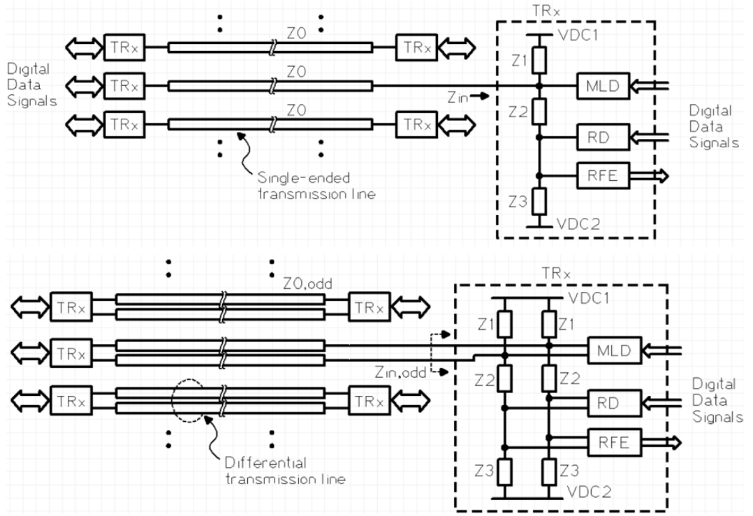
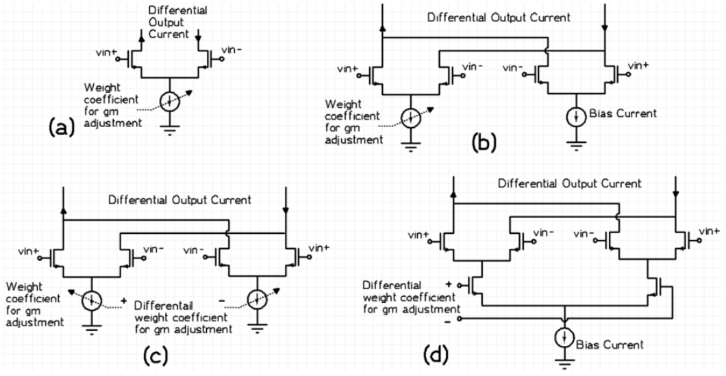
Figure (1) Illustration of self-interference and echoes in multi-lane interconnects; (2a) Illustration of RD based transceiver frontend for SI/echo/crosstalk cancellation with single ended transmission lines, (2b) Illustration of RD based transceiver frontend for SI/echo/crosstalk cancellation with differential transmission lines; (3) Illustration of few examples of Gm cells with NMOS transistor implementation with differential outputs
Modern high-speed communication systems increasingly demand simultaneous bidirectional signaling over shared interconnects to reduce pin count and improve bandwidth density. However, implementing this in a compact form factor faces major challenges. Self-interference from the device’s own transmitter, echo from impedance mismatches, and near-end crosstalk from adjacent data lanes severely degrade signal quality. Conventional solutions such as passive hybrids or digital cancellation techniques are bulky, power-hungry, and not scalable for on-chip or chip-to-chip interconnects. Therefore, there is a pressing need for a compact, power-efficient, and circuit-level solution that can enable full-duplex signaling without sacrificing signal integrity.
- Ratioed Driver-Based Cancellation: This technology injects weighted and delayed replicas of transmitted and adjacent-lane signals to cancel SI, echo, and NEXT at the receiver input.
- Adaptive Weight Tuning: It enables dynamic control of injected signal strengths for optimal cancellation.
- Integrated Circuit Design: The circuit is suitable for on-chip or chip-to-chip integration in dense packages.
- Power and Area Efficient: This avoids large passive elements and complex digital cancellation blocks.
- High Data Rates Supported: This invention enables simultaneous bidirectional transmission, reducing the number of wires needed to achieve a certain data transfer rate across the interconnect.
The prototype consists of a custom CMOS test chip demonstrating simultaneous bidirectional data transfer over a single wire. It includes ratioed drivers on both ends to inject calibrated cancellation signals and shared-wire interconnects designed to support high-speed, low-power communication. High-sensitivity receivers and tuning modules are used to manage echo and crosstalk, ensuring signal integrity.
A semiconductor chip based prototype has been demonstrated.
4
As computing moves toward more intelligent, high-performance, and decentralized systems, efficient data communication within and between chips becomes foundational. This invention directly supports this evolution by enabling faster, more compact, and energy-efficient communication links. The technology can lead to greener data centers, lower-cost AI hardware, and more accessible consumer devices, thereby promoting energy sustainability, digital equity, and technological innovation across society.
- High-speed chip-to-chip and die-to-die interconnects
- AI/ML accelerators and data-intensive processors
- High-performance computing and supercomputing systems
- Data center networking and cloud infrastructure
- Advanced networking equipment (switches, routers)
- Compact consumer electronics and mobile SoCs
Geography of IP
Type of IP
202321026913
564078