This invention presents a novel active current source gate driver (ACSD) for improving the switching performance of silicon carbide (SiC) MOSFETs. The proposed driver provides a constant current during the switching transitions which allows the fast turning on and off of the semiconductor device. One of the major concerns due to the fast switching of these devices is the generation of high dv/dt and di/dt. Furthermore, its interaction with the circuit parasitic results in severe oscillations, overshoots and EMI. The ability of the proposed ACSD to allow the gate voltage decrement for short time can provide control over the current and voltage slew rates. The reduction in the voltage and current slopes further suppress the overshoots, oscillations and limits the EMI when compared to the conventional gate drivers. This invention presents the detailed operation of the proposed ACSD and is also experimentally verified by performing double pulse tests (DPT). A reduction in overshoot of 30% and 32% in voltage and current is observed with reduced oscillations. Further, the frequency spectrum obtained proves the efficacy of the proposed ACSD in achieving low EMI.
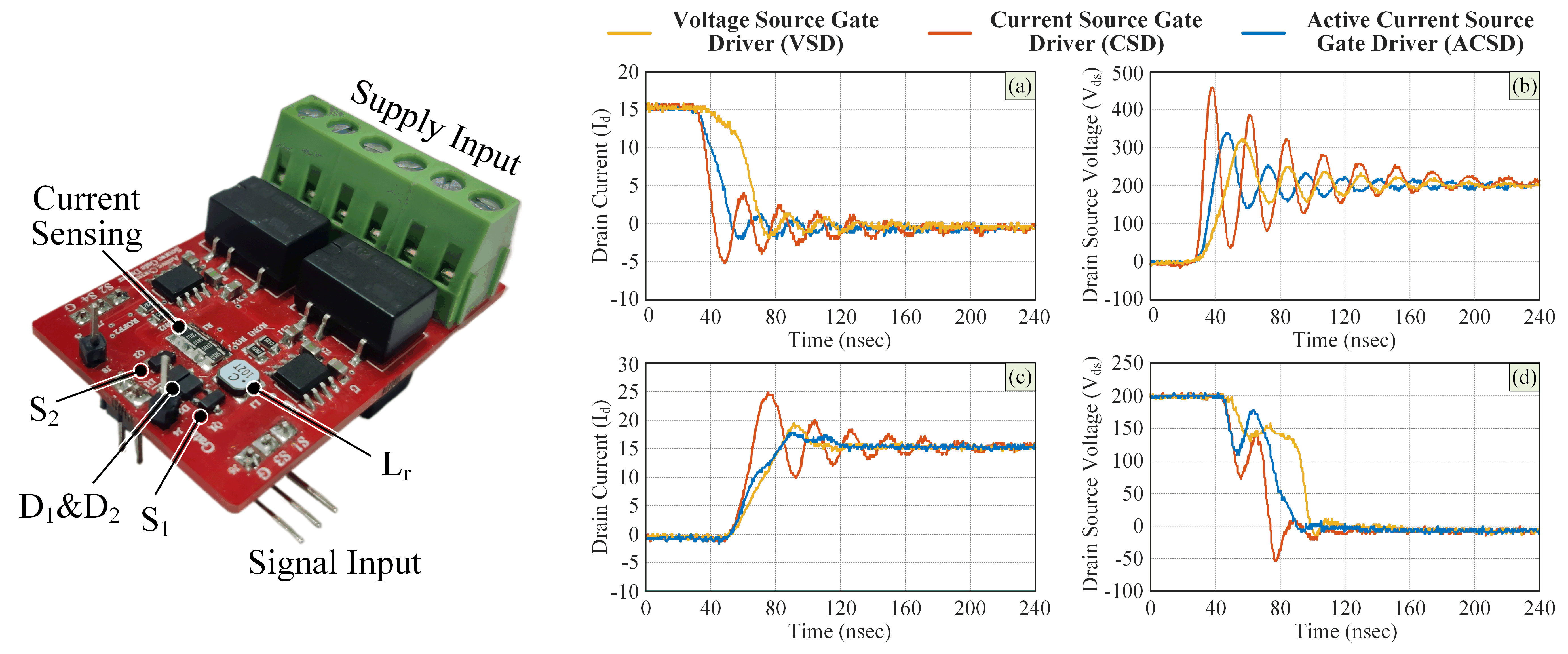
Figure 1. Key switching waveforms of all the considered cases (a) Drain current, (b) Drain-source voltage during turn-off switching transition, (c) Drain current and (d) Drain-source voltage during turn-on switching transition
The conventional voltage source gate driver limits the switching speed and also leads to increased switching losses. On the other hand, the current source gate driver achieves faster switching transition. The fast switching of the power semiconductor devices allows for higher dense converter, but also results in high slew rate (dv/dt and di/dt), which leads to overshoots and oscillations. This further results in conductive and inductive EMI.
In this invention, we have come up with a new technology defined as active current source gate driver. The proposed invention features the ability of the current source gate driver, and the gate voltage decrement feature enables the control over the slew rate. Hence, the proposed solution achieves lower switching losses along with reduction in overshoots, oscillations and EMI.
- Reduced and Controlled Slew Rates (dv/dt and di/dt): The gate voltage decrement features provide controlled gate voltage.
- Efficient Switching: It has high switching frequency capability with reduced losses.
- Low EMI: The reduces oscillations in the device voltage and current will lowers the occurrence of EMI in the circuit.
- Semiconductor Switches: All applications use power semiconductor switches such as MOSFETs, IGBTs.
Prototype has been developed and validated.
A reduction in overshoot of 30% and 32% in voltage and current is observed with reduced oscillations.
3
The proposed solution can provide a drastic reduction in losses in the power converter. Also, the current source ability allows the faster switching and leads to high power dense solution.
- Semiconductors Devices and Power Electronic Converters Manufacturing: Driving any power semiconductor switches such as MOSFETs and IGBTs
Geography of IP
Type of IP
202121000857
493290