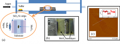
Despite a tremendous interest on molybdenum disulphide as a thinnest direct band gap semiconductor with a huge potential for application in optoelectronics and plasmonics, single step synthesis of a large area purely monolayer MoS 2 film has not yet been reported. We have adopted a chemical vapour deposition (CVD) route to synthesise a continuous film of strictly monolayer MoS 2 covering an area as large as several mm 2 on a variety of different substrates without using any seeding material or any elaborate pre-treatment of the substrate. This is achieved by allowing the growth to take place in the naturally formed gap between the pieces of SiO 2 coated Si wafer and the substrate, when the latter is placed on top of the formers inside a CVD reactor. In this process, the gap that is formed between the substrate and the wafer, acts as a natural reactor cavity, resulting in the formation of continuous MoS 2 monolayer, occupying the entire region of the substrate covered by the wafer. The highlight of this method is that it results in the synthesis of strictly monolayer films. Multiple layers have never been found in any of the samples grown by this technique, even when the samples are grown with a wide range of growth parameters. This result is thus a significant step forward for the realisation of MoS 2 monolayer based integrated devices, which can utilise certain unique features of this 2D semiconductor. Moreover, this particular technique could be extended for the growth of other 2D dichalcogenide semiconductors such as WS 2 , MoSe 2 and WSe 2 .
Prof. Subhabrata Dhar