SNOM (Scanning Nearfield Optical Microscopy) – Nano Nics
NSOM (Near-field Scanning Optical Microscopy), sometimes referred to as SNOM, is the premier tool for imaging and manipulation of light on the nanoscale. It is the only super-resolution optical method that captures the near-field of light distribution, allows for all forms of optical imaging, correlates light distirbution with topography, and is effective in all environments.
Nanonics offers instrumentation for unlimited NSOM, thereby enabling a broad set of applications for NSOM, both apertured and apertureless near-field imaging. In addition, Nanonics has pioneered multiprobe NSOM platforms that are effective for pump/probe optical transport phenomena on the nanoscale. Open new frontiers with this paradigm shift in super-resolution imaging in the 50-100nm range that allows investigation of both surface and near-surface phenomena.
Modes of Operation: Aperture less, Reflection, Collection, Transmission, Fluorescence, Raman, Nano illumination SNOM.
The invention of AFM introduced the ability to characterize samples with a wide variety of techniques at the nanoscale, now comes the next evolution of MultiProbe AFM. With the ability to employ a wide variety of SPM probes nanometers from each other, transport scales can be studied on the nanoscale with a flexibility and ease not available before. This state of the art instrument offers nanoscale transport measurements for optical, electrical, and thermal measurements. Or use a high resolution AFM probe with another dedicated SPM probe to get the highest AFM resolution in every SPM measurement. With full optical integration the MV 4000 is a real workstation for nanoscale characterization.
The power of independently controlled multiprobe AFM with all SPM modes is exclusively and only available today in the Multiview 4000. As many as four probes operate simultaneously and independently, each with feedback and scanning capabilities. Measure sophisticated properties only possible with multiple probes such as electrical, thermal and optical properties of devices. The Multiview 4000 is a novel and only platform containing multiple probes/AFMs for advanced experiments such as: nanoscale transport, optical pump-probe, and read-write experiments. The Multiview 4000 continues the tradition of the Multiview series, providing total optical flexibility and customization possibilities. Now, AFM Raman and Tip Enhanced Raman Spectroscopy (TERS) can be integrated with multiprobe capability. In addition, free optical access from above allows easy visualization of all probes and facilitates nanomanipulation.
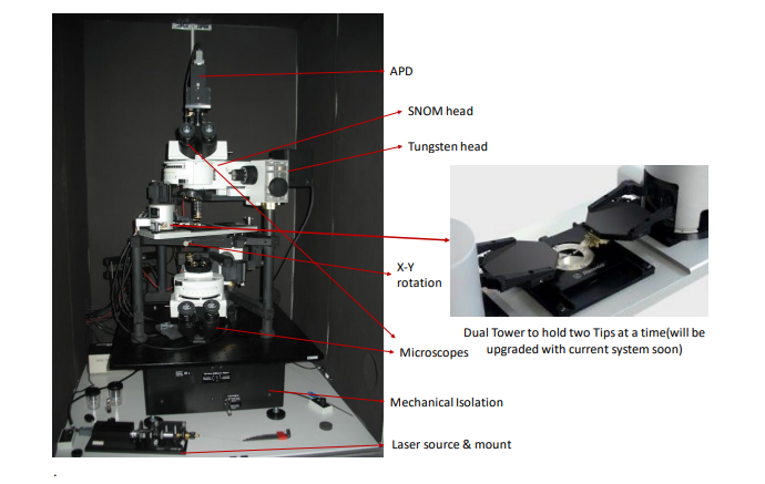
Characteristics: Dual Optical Microscope(Olympus) working in up-right and inverted mode with mechanical isolation; Confocal Microscopy facilities; Nano Fountain Pen for writing and chemical delivery and removal at the nanometer level; Imaging resolution for NSOM: 50 nm, AFM: 20 nm; Scanner resolution: <0.05 nm (Z) and <0.15 nm (XY).
SNOM Modes
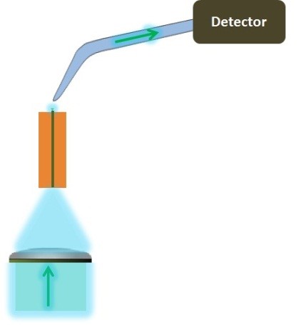
True Collection Mode
Collection mode NSOM is depicted in the schematic below, where the light illuminates the sample, and then is collected through the NSOM probe by a detector. The MultiView 4000 offers both tip scanning and a sample scanning stage with upto four probes that can scan independently and simultaneously. A sample scanning stage enables easy and rapid alignment of the sample relative to the illumination source and ensures that the microscope optics are independent of the AFM scanner. This instrumentation design is ideal for true collection mode NSOM.
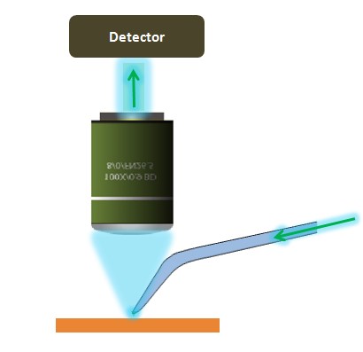
True Reflection Mode
In true reflection mode, light is introduced via the NSOM probe, and then collected by a detector above the probe as shown in the schematic below. True Reflection mode NSOM is possible on the MultiView 4000 due to the use of transparent, cantilever probes. Furthermore, the design of the MultiView series separates the excitation and collection paths so that they don't affect each other, thus enabling true reflection mode NSOM measurements to be conducted. Other designs that take advantage of straight probes or apertured Si probes are significantly more challenging for true reflection mode.
Simultaneously Characterize Multiple Dimensions
The simultaneous and independent SPM probe operation of up to 4 probes enables full characterization of all dimensions of samples and devices. All forms of SPM are enabled for each individual probe accompanied by total optical integration resulting in access to all modes including AFM, KPM, EFM, ANSOM, NSOM, STM, AFM-Raman, and TERS. Because these probes are designed for multiple probe operation, they can be brought to a nanometric separation distance thus ensuring that the same area is scanned with all the probes.
AFM, CFM (with the atmosphere), KPFM (with the atmosphere), SNOM, Fluorescence
Probe Station for Electrical Measurements
Multiprobe capability is especially useful for electrical measurements since multiple probes can now be placed over the element to provide bias or probe its conductivity, resistance, etc just like in a probe station. Two-, three-, or four-point resistance measurements are possible. Multiple probes also enable flexible positioning and manipulation to provide bias, localized I-V measurements, and multichannel imaging.
Integrate SPM Modes with Topography
With a multiprobe system, resolution and tip quality no longer need to be compromised since each probe is now individualized for each measurement. In classic NSOM setups the NSOM probe would have the dual function of imaging topography and fluorescence where the topography image is compromised by the aperture (wider diameter) needed by the NSOM probe. But in a multiprobe setup, a standard SPM probe can be used the topography without affecting the NSOM fluorescence measurement.

The left and center images are the topography and fluorescence images, respectively, of lumogen dye particles collected in a multiprobe setup with different probes for topography and NSOM. The image on the right is the topography image of the same sample but collected with the NSOM probe, revealing the clear loss of resolution and morphology. The width of each image is 8um.
Nanoscale Transport
One probe can be the source of excitation while the second probe follows the transport process with high spatial resolution. Alternatively, optical pump/probe experiments can now be performed using one probe to optically pump while the other probe measures the optical output in a variety of configurations. An example of each type of measurement is shown below.
1. Thermal transport measurement within an SRAM device where heat is introduced at specific locations and detected at other locations. As contact is made in different regions of the SRAM with the thermal conductivity probe, the probe tip cools to different levels depending on the material's thermal conductivity. The resulting image is obtained by determining the current alterations that had to to be affected in order to keep the current flowing past the point resistance at a constant value.
2. With two cantilever, near-field optical probes with exposed tips, light is injected through one probe and is guided through the sample which is a fiber. With the second probe in place, this injected light can be collected and analyzed both spatially and temporally. In this image two NSOM probes are seen in AFM contact with the input and output of the fiber waveguide.
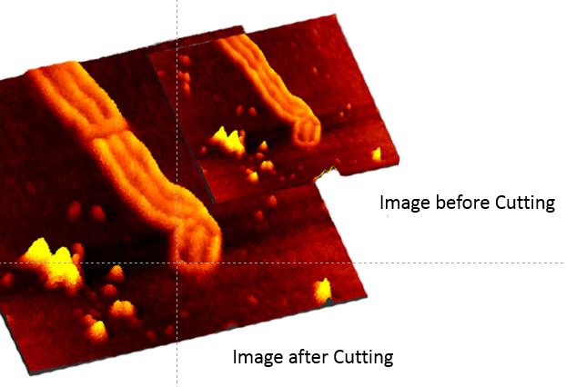
Nanoscale Manipulation and Measurement
One probe can be used for moving, cutting, or positioning a sample, while the other probe can be used to image the sample. For example, shown below is a chromosome that has been dissected with one probe (see image on left), while the other probes images the result of the nanomanipulation.
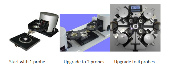
Modular Design for Easy Upgrade
The unique, modular design of the MultiView 4000 allows for the upgrade from one probe to two, three or four probes.
Unique 3D Flatscan Scanner Technology
The design of the 3D Flatscan is a novel planar, folded-piezo flexure scan design that keeps the probes separated. The large vertical (axial) displacement of up to 100 microns allows for the use of multiple probes as well as the tracking of structures with very large topographical features. The minimal scanner height of 7mm allows for easy access with high powered microscope objectives from either above or below the scanning stages.
Spatially Friendly Glass Probes
While typical probes do not permit close proximity of probe tips, Nanonics has developed spatially and optically friendly glass based probes that allow for a close approach of the probe tips to within nm, as well as independent scanning of each probe. Nanonics' glass based probes offer excellent imaging in AFM modes, unparalleled aspect ratios, and support deep trench imaging as well as side wall imaging. They also permit singular electrical imaging and thermal imaging with glass encased nanowires.
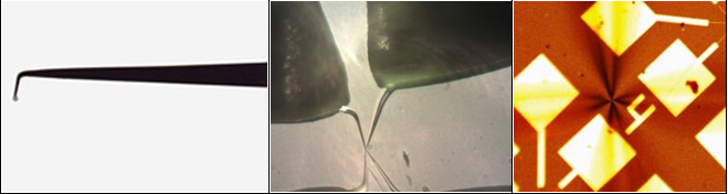
Left: Nanonics' patented bent cantilevered glass probe
Center: Online dual probes in contact with AFM feedback (side view)
Right: Online four probes in contact with AFM feedback (top view 500x magnifications)
Ultra-sensitive Tuning Fork Feedback
Easy to use and ultimate force sensitivity with tuning fork feedback allowing soft approach of probes to one another for ultra-close positioning. For a further explanation of this feedback mechanism, see our Tuning Fork Tutorial.
Tip & Sample Scanning Options
The MultiView 4000 provides both tip and sample scanning so that the user can select which mode of operation best suits their experimental needs. For example, a sample scanning stage enables easy and rapid alignment of the sample relative to the illumination source and ensures that the microscope optics are independent of the AFM scanner. On the other hand, the tip scanning stage means that the tip can be scanned while the illumination point is held constant.
Free Optical Axis from Above the Probe
The MultiView 4000 offers a completely free optical axis from above the probe, below the sample and 270 degrees around the probe. The Multiview 4000 boasts a 4.5mm working distance from above the probe for ultrahigh-resolution optical or electron/optical viewing probes on opaque samples.
1. Failure analysis of microchips and chemically mechanically polished microchips
- Generate carriers locally using optical capabilities of NSOM without need for electrical connections.
- Light emission from working devices.
- Kelvin probe measurements with and without light injection.
- Integrate potential difference or photovoltage measurements with optical capabilities of NSOM tip.
- Use our optical fiber probe and significantly reduce electrical effects due to the metallic cantilevers in conventional AFM systems.
- Place Nanonics NSOM/AFM 100 on any conventional upright microscope and view tip positioning relative to the sample from directly above through microscope objective. Conventional AFM cantilevers obscure the tip, which sits under an opaque material, and thus cannot be used with a conventional upright microscope.
- Capacitance measurements of gate oxide leakage and dopant concentration.
- Direct correlation of all of the above. Direct registration of simultaneously obtained near-field optical images and AFM images that clearly show that the oxide layers have not been removed and that the NSOM and simultaneous electrical measurements are probing the structure beneath the overlying oxide.
- Fowler-Nordheim oxide thickness measurements exactly overlapped with oxide surface structure.
- Simultaneous NSOM resistivity measurements. For example, correlating resistivity in the titanium salicide layer with overlaid NSOM optical imaging or pn junction resistance with optical imaging through an oxide.
- Correlation of resistivity and optical reflectivity of surfaces.
- Correlation of capacitance, optical reflectivity, and AFM at the same resolution for investigating gate oxide leakage or ensuring the leakage is through an oxide layer and not just surface exposure.
2. Polymer Imaging (NPLM-Near-field Polarized Light Microscopy)
- NPLM characterization of polymer microdomain structures; correlation with polymer chemistry.
- Simultaneous far-field polarized light confocal microscopy and NPLM additional data on polymer topography and elasticity. This category of simultaneous imaging can be done by no other AFM system today. All of these systems which use silicon cantilevers block the point at which the tip is interacting with the sample and therefore no optical imaging can be done at the tip. In addition, no lens can be brought above the tip for the far-field transmission polarized light microscopy because the feedback of silicon cantilevers requires the z control light beam mechanism to be brought directly above the cantilever in other AFM systems.
- An important aspect of polymer microdomain structure is the fact that it is related to polymer crosslinking, which is a very important parameter in polymer chemistry and physics. The Nanonics system is able to effectively image such structures.
3. Telecommunication and Optoelectronic Devices
- Characterizing waveguides, semiconductor diode lasers, microlasers, semiconducting polymers, and solid-state materials.
- Measuring optical distribution of light and mode structure at different emission wavelengths of waveguides and microlasers. Correlating this information with electrical properties of the devices, both on a macro scale and on a micro scale, by using the NSOM tip for monitoring carrier distribution and injected charge.
- Measuring the thermal distribution in such devices.
- Electric optical switching devices.
- Polymer electro-luminescence – either collect or inject light and measure electrical properties of devices made of such materials.
- Porous silicon.
- Gallium Nitride lasers.
- Measuring light distribution in electro-optically active crystals as a function of injection of electrical charge.
- Optical fiber and optical waveguide switches characterization.
4. Applications in Bacteriology
- Staining nucleic acids and proteins in bacteria and measuring distribution of specific proteins and DNA and RNA in bacteria.
- Bacterial imaging without staining using specific laser wavelengths, such as in the DNA absorption at 266nm.
- Correlating the previous two measurements with the bacterial life cycle.
5. 3D Optical Microscopy/NSOM/AFM Combination
- Correlating a CCD digital optical image, a confocal image, or a non-linear optical image obtained through a microscope with NSOM and AFM data at specific points.
- Use this NSOM and AFM data as super-resolution constraints for mathematical deconvolution algorithms that rapidly de-convolve the entire 3D optical image at resolutions unachievable with lens-based far field microscopy.
6. Biotechnology
- AFM based topographic structure and simultaneous NSOM chemical structure identification by optical staining. On-line correlation of all this data with far field optical images.
- Dissection of specific regions of chromosome correlated with the previous measurement and sequence identification of these regions by the application of PCR technology.
- Relationship of mechanics of specific regions using AFM capabilities with optical imaging (NSOM and far field) of stained DNA and the dissected chemical structure. Investigation of the nature of fragile sites.
7. Laser Tweezer/AFM Combination
- Correlating laser tweezer forces with AFM detected forces in nano-regions.
8. Gold or Silver Ball Immuno-Labeling Antibody Attachment to Specific Proteins
- Competitive use of NSOM instead of electron microscopy in pathology laboratories and in investigations of gold and silver labeled biological tissue and sectioned biological tissue, such as brain slices for monitoring neuronal interconnections. In addition, live tissue investigations with such staining are possible.
9. Optical Ion Sensing
- Ion sensing around membrane channels with NSOM and force sensing of sub-nanometer protein and membrane movements.
- NSOM/Ion conductance/AFM.
- NSOM focal uncaging of neurotransmitters and other molecules for the investigation of synaptic function and plasticity.
- Ion conductance using a multi-channel AFM/optical fiber probe for simultaneous measurements of membrane ion conductivity, channel movement, and optical signals, such as fluorescence of fusing synaptic vesicles, local fluorescence near membrane, and intracellular ion sensing dyes.
- Full correlation of all of the above with far field optical confocal or non-linear optical fluorescence imaging and evanescent wave microscopy.
10. Fountain Pen Force Sensing Applications
- Chemical writing with single or dual channel nanopipettes.
- Selective etching with gases or liquids.
- Flat panel display correction.
- Tribology with specific lubricants in the fountain nanosensor monolayer deposition.
- Crystal growth with mother liquor in one channel and ion sensing in the other channel using NSOM. To understand the underlying mechanisms that lead to crystal growth, it is crucial to know the ionic environment at and above a specific crystal plane as it grows. When this is coupled to the ability of chemical sensors (also manufactured by Nanonics) to measure surface forces, one obtains a multidimensional view of crystal growth that has never before been achievable. This should lead to new views of how crystals grow and how to coax the growth of crystals, from those associated with small molecular systems to biological macromolecules.
- Lipid deposition in specific membrane domains with lipid tip coated/force sensing cantilevered nanopipettes.
- Simultaneous capillary electrophoretic delivery of chemicals to cells and with AFM sensing.
11. Photoresist Exposure in the UV, Deep UV (193nm) and Ultra Deep UV (157nm)
For photoresist development and characterization in the microelectronics industry.
12. Data Storage Applications
- Magneto-optic investigations.
- Etching structures for data storage investigation.
- Optical / AFM integration - optical alterations with AFM detection.
13. NanoRaman, Nano IR, Nano-Two Photon, and Nano-Second Harmonic Spectroscopy
- Apertureless enhancement in nanoregions with unique glass cantilevers nanotipped with a silver particle of controlled size, from two to hundreds of nanometers.
14. Nano-Aperture Based Infrared Application
- Local heating for micro-soldering.
- Collection of infrared light for monitoring light distribution in quantum cascade lasers (see also 2 above) and correlating this information with electrical properties of such lasers.
- Vibrational spectral imaging of single molecules and their films.
15. Thermal Sensing Cantilevered Tips with Optical Sensing 16. Scanning Electro-Chemical Microscopy
- Using multi-channel cantilevered glass tips to perform simultaneous electrochemical and near-field optical imaging. Fully correlated with far-field optical microscopy.
17. Ultra-Fast Laser Spectroscopy and Surface Modifications
- Femtosecond pulse delivery in nano-regions.
- Pump-probe spectroscopy. For example, carrier injection in semiconductors together with force sensing techniques.
- Femto-second lithography of metals and metallic structures without associated heating.
18. Monitoring Optically Induced Dynamic Structural Alterations in Proteins, Membranes, and Chalcogenides
With microsecond time resolution.
19. Fluorescence NSOM/Confocal Imaging
- Single molecules, nanocrystals and thin films with and without imposed forces, electrical fields, etc.
- Cellular fluorescence imaging.
- Prof. Dinesh Kabra
HOD -324, Department of Physics, I.I.T. Bombay, Powai, Mumbai - 400076
Contact No: 022-2576-6568
- Dr. Saleem Shaik (Operator)
- Mr. Suryanarayan Nayak (On behalf of Operator)
Prof. Dinesh Kabra
Prof. C Subramaniam
Prof. Subhabrata Dhar
Dr. Pramod Kumar
Dr. Abhijeet Sangle