A simple, low-cost way to make tiny, upside-down pyramids on silicon surfaces to help solar panels catch more sunlight. Instead of using complex light-patterning steps, it lays down a thin coating, heats it so natural bubbles form, and then dips the silicon in a safe chemical bath. The bubbles act like tiny stencils—wherever a bubble sits, the chemical carves in a little pyramid. This method has been proven in the lab and can be added to existing solar cell lines with almost no extra equipment.
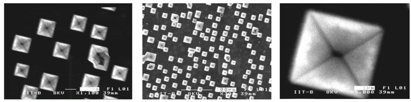
Figure 1. SEM micrographs showing formation of inverted pyramidal structures on silicon.
Making high-efficiency solar cells often needs a complex and expensive process called photolithography, which includes several steps and chemicals. This makes solar cell production costly and less eco-friendly. There is a strong need for a simpler, cheaper, and more environmentally friendly method to improve the performance of solar panels without using this traditional technique.
- Product Uses Natural Bubble Masks: Instead of painting patterns, this feature harnesses tiny blisters that form naturally on a thin coating when heated. The bubbles become removal points, guiding the etching chemical to carve inverted pyramids.
- Feature Boosts Sunlight Capture: By creating uniform, microscopic pyramid pits, the inverted shapes trap more sunlight inside the silicon, improving electricity output without extra materials.
- Advantage Integrates Easily: There's no need for new expensive machines—just add a coating step and a heat cycle to existing solar panel lines. Minimal training and no major capital upgrades are required.
- Feature Cuts Chemical Waste: It eliminates photoresist inks, developers, and their disposal. Only common, easier-to-handle chemicals are used, reducing hazardous waste and boosting sustainability.
In the lab, researchers coated small silicon samples with a thin silicon-nitride film, then heated them between 400°C and 900°C. Scanning-electron microscope images confirmed clear bubble-formed masks and well-shaped inverted pyramids sized 5–20 μm. Etching was done in a warm (70°C–90°C) solution of potassium hydroxide, followed by a quick film-removal bath.
The process has been successfully tested in laboratory conditions, where small samples of silicon were treated using this method. Clear results showed the formation of the required pyramid shapes, and images taken under special microscopes confirmed the structure.
4
By cutting production costs and boosting efficiency, this method makes solar panels significantly more affordable, which can translate into noticeably lower electricity bills for households, businesses, and schools. Dropping the need for harsh photolithography chemicals not only slashes manufacturing waste but also reduces exposure to dangerous substances, creating a safer workplace and lessening environmental pollution. In remote or underserved communities, these lower-cost panels can deliver dependable power for lighting homes, preserving vaccines in refrigeration units, and keeping communication networks online. This expanded access to clean energy can foster economic growth, improve healthcare delivery, and extend learning opportunities long after sunset.
- Solar panel manufacturing: Fabricating and assembling photovoltaic modules for electricity generation
- Semiconductor surface texturing: Creating micro- and nano-scale patterns on silicon wafers to modify surface properties
- Renewable energy production: Generating power from sustainable sources like solar, wind, and hydro
- Sustainable materials processing: Developing eco-friendly methods to produce and treat industrial materials
Geography of IP
Type of IP
132/MUM/2013
374367