This invention describes a method of synthesizing a target material using an ultrafast laser ablation technique. The method includes impacting a target material immersed in a suitable solvent with an ultrafast laser light and ablating a portion of the target material. The method also includes repeating the ablation in a plurality of portions of the target material. Further, the method includes forming two dimensional (2D) sheets of a hexagonal shaped 2D lattice of the target material.
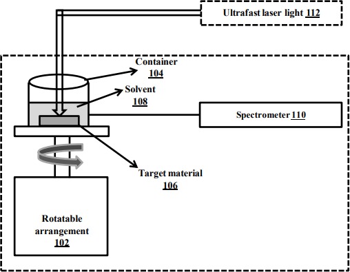
Figure 1. Illustration of a system of synthesizing a target material using an ultrafast laser ablation technique
Conventional methods for synthesizing 2D materials like graphene and its analogues often involve complex processes, high temperatures, or hazardous reagents, causing defects and limited scalability. Bulk Group IVA materials have crystal structures different from the desired hexagonal lattice of their 2D forms, making it hard to produce large-area, high-quality nanosheets with uniform atomic arrangements. Thus, there is a need for a simple, clean, scalable technique to transform bulk Group IVA materials into high-purity 2D sheets with hexagonal lattices, while minimizing thermal damage and enabling easy separation from nanoparticles.
- Ultrafast Laser Ablation Technique: The method utilizes femtosecond laser pulses focused through a 10 cm focal length lens to ablate bulk Group IVA materials immersed in a suitable solvent, enabling precise control over the synthesis process.
- Hexagonal Lattice Formation: Unlike conventional methods, this process induces atomic rearrangement to form 2D sheets with uniform hexagonal lattice structures, even when starting from bulk materials with different crystal structures.
- Clean and Green Process: The method avoids the use of hazardous chemicals and high-temperature treatments, significantly reducing environmental impact and potential contamination of the final product.
- Scalable and Versatile: The setup includes a rotatable container allowing uniform laser exposure on multiple portions of the target material, facilitating scalable production of large-area nanosheets across various Group IVA elements (graphene, silicene, germanene, stanene, plumbene).
- Efficient Separation of Nanostructures: Post-ablation, the method leverages centrifugation to separate thin atomic layers suspended in the solvent from nanoparticles, ensuring high-purity sheets suitable for advanced applications.
- High Structural Quality and Purity: Characterization techniques such as HRTEM, SAED, Raman spectroscopy, and EDX confirm the formation of defect-free, high-quality 2D materials with minimal impurities, enhancing their suitability for electronics, sensors, and other cutting-edge technologies.
The prototype includes an apparatus for synthesizing high-quality 2D sheets of Group IVA materials using ultrafast laser ablation. It features a rotatable holder for a container with the target material immersed in a suitable solvent, enabling uniform laser exposure and reducing thermal effects. A 10 cm focal length lens focuses ultrafast laser pulses onto the rotating target (20 rpm) for consistent ablation. The process produces nanosheets with hexagonal lattices suspended in the solvent, which are separated from nanoparticles by centrifugation. The system also integrates spectrometers and other components to monitor and control the synthesis.
This method is at demonstration and/or validation stage in lab environment.
4
The development of a clean, scalable, and efficient method to synthesize high-quality 2D materials promotes sustainable manufacturing and enables widespread use in electronics, energy storage, sensors, and healthcare. By avoiding hazardous chemicals and reducing environmental harm, this technology supports innovation in next- generation devices, leading to improved performance, energy efficiency, and economic growth across industries, ultimately enhancing quality of life and fostering a greener future.
- Nanoelectronics: Transistors, sensors, flexible electronics
- Energy storage and conversion: Batteries, supercapacitors, solar cells
- Optoelectronics: Photodetectors, LEDs
- Catalysis: Due to high surface area 2D sheets
- Material science research: New 2D materials for fundamental and applied studies
- Biomedical applications: Biosensors, drug delivery platforms
Geography of IP
Type of IP
3253/MUM/2015
431134