This invention describes a method for fabricating passive polymeric structures of sub-wavelength dimensions. The method includes preparing an acrylate mixture, where the acrylate mixture comprises of acrylate monomers and a photo initiator. Further, the method includes spin coating the acrylate mixture over a transparent substrate and patterning the transparent substrate using two photon lithography by irradiating the coated transparent substrate with a laser source. Further, the method also includes removing un-polymerized acrylate mixture to obtain free standing polymeric structures of sub-wavelength dimensions.
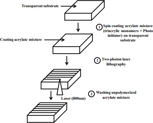
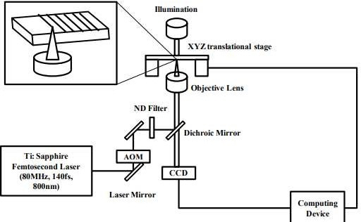
Figure (1) Method for fabricating a passive polymer of sub-wavelength dimensions using a dyeless two photon lithography technique; (2) Method for performing two photon lithography using a laser source for patterning on a transparent substrate
Current 3D microfabrication techniques for micro-optics, photonics, and biomedical devices often face challenges such as high laser power requirements, limited resolution, slow processing speeds, and high costs. These limitations hinder the efficient production of precise, miniaturized, and complex microstructures necessary for advanced applications in microfluidics, optical components, tissue engineering, and flexible electronics. There is a need for a cost-effective, high-resolution, and faster microfabrication method that reduces energy consumption while enabling reliable and scalable fabrication of intricate 3D microstructures.
- High-Resolution 3D Microfabrication: The technology achieves ultra-fine feature sizes down to approximately 200 nm by leveraging precise two-photon polymerization techniques, enabling the creation of highly detailed and intricate micro- and nanostructures suitable for advanced applications.
- Optimized Photoinitiator Efficiency: It employs lucirin-TPOL as a highly efficient photoinitiator that produces a significant number of free radicals even at reduced laser power levels, resulting in lower energy consumption and improved polymerization efficiency.
- Enhanced Fabrication Speed: It enables increased writing speeds by reducing the polymerization threshold power, which improves throughput while maintaining high resolution and structural integrity of the fabricated patterns.
- Precise Control over Pattern Dimensions: It provides the ability to finely tune line widths and polymerization quality by adjusting the concentration of photoinitiator and laser parameters, allowing for customizable and reproducible microstructure fabrication.
- Complex Multilayer and 3D Structure Fabrication: It supports single-step fabrication of complex multilayer and three-dimensional architectures directly on transparent substrates, expanding possibilities for creating sophisticated micro-optical and biomedical devices.
- Cost-Effective and Scalable Process: It integrates reduced laser power requirements with efficient polymerization kinetics, lowering operational costs and enabling scalable manufacturing suitable for various industries including photonics, microfluidics, and flexible electronics.
The prototype consists of a novel photoresist formulation with lucirin-TPOL photoinitiator and acrylate monomers optimized for two-photon polymerization using an 800 nm laser, enabling high-resolution 3D microfabrication with feature sizes down to ~200 nm, demonstrated by complex microstructures like stepped pyramids and multilayer meshes on transparent substrates. Operating at reduced laser powers and faster scanning speeds, it offers precise control over polymerization thresholds and line widths. SEM imaging confirms well-defined polymer lines and multilayer 3D structures, validating the technology’s effectiveness and versatility for advanced microfabrication applications.
The technology is at demonstration and/or validation in lab environment stage.
4
This technology enables significant advances in micro-optics, photonics, and biomedical devices by providing precise and cost-effective 3D microfabrication. It has the potential to accelerate the development of customized microfluidic devices, optical components, and tissue engineering scaffolds, while also supporting the creation of next-generation sensors and flexible electronics with enhanced miniaturization. Additionally, by lowering laser power requirements and reducing processing times, it may help decrease production costs and minimize the environmental footprint of microfabrication processes.
- Microfabrication and nanomanufacturing
- Photonics and optical device fabrication
- Biomedical engineering and tissue scaffolds
- Microfluidics and lab-on-chip devices
- Sensor technology and electronics
Geography of IP
Type of IP
201821042628
479963