The present invention relates to a device that utilizes oscillation of electrons in metals for manipulating electromagnetic radiation. The device is capable of concentrating electromagnetic energy at a focal spot with an intensity of almost 3.5 times more than incident wave. A multifold enhancement in the efficiency of currently existing devices is thereby possible, when incorporated with the device. The device also demonstrates achromatic behavior and it gives it an additional advantage of focusing all wavelengths at same focal spot, within operating range of device spatially. The plasmonic lens can be easily fabricated using existing lithographic techniques, so is compatible with existing cMOS based technologies. Further, the focal length of the device can be tuned from 2 μm to 18 μm. The device is optimized for 400–700 nm region but the same can be expanded to entire uv-vis-NIR region of the spectrum allowing a tremendous increase in the efficiency of all the devices.
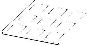
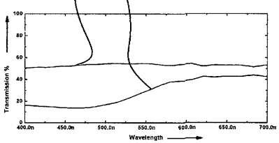
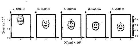
Figure (1) Depiction of a three-dimensional view of a third periodic device; (2) A graphical illustration of transmittance and reflectance curve from wavelength ranging from 400 nm to 700 nm of the third periodic device; (3) Depiction of the normalized electric field for incident wave energies with wavelengths from 400 nm to 700 nm on the X-normal cross-section of each aperture in the third periodic device.
Conventional microlenses suffer from chromatic aberration, where different wavelengths focus at different points, leading to poor focusing performance across the visible spectrum. Furthermore, achieving subwavelength focusing with high intensity and minimal energy loss in compact form factors remains a significant challenge in micro-optics and photonics, especially for super-resolution imaging, photodetectors, and optical sensors.
- Achromatic Broadband Focusing: The microlens effectively focuses light across a wide visible spectrum (400–700 nm) with minimal chromatic aberration, maintaining consistent focal performance across varying wavelengths.
- Dielectric-Metal Multilayer for Surface Plasmon Excitation: Utilizing a transparent dielectric layer paired with a metal layer (e.g., gold), the device excites surface plasmon polaritons at the interface to enhance light manipulation and nano-focusing capabilities.
- High-Intensity Nanoscale Light Concentration: The design concentrates incident light into nanoscale focal spots with significant intensity enhancement (up to 3.3×), essential for applications requiring precise and strong localized illumination.
- Tunable Focal Length and Depth with Symmetric Emission: Focal length and depth decrease predictably with increasing wavelength, allowing wavelength-specific optimization, while symmetric structure ensures uniform electric field distribution in both principal planes.
- Customizable Aperture Geometry for Optimized Diffraction: The microlens features various aperture shapes (square, circular, star-shaped) with intersecting arms, enabling tailored diffraction and interference patterns for improved light concentration and device versatility.
- Material and Array Configuration Flexibility: The metal layer can be composed of various metals (e.g., gold, silver, aluminum), offering fabrication adaptability, while periodic aperture arrays allow scalability and multiple focal spot generation for broader optical integration.
The proposed technology addresses the problem of chromatic aberration and limited subwavelength focusing in conventional microlenses by introducing an achromatic, plasmonic metal-dielectric microlens capable of maintaining consistent focal length and high-intensity performance across the visible spectrum (400–700 nm). Utilizing surface plasmon polariton excitation at the metal-dielectric interface, the microlens achieves deep subwavelength focusing (as small as 80 nm × 80 nm) and intensity enhancement factors (Zp) up to 3.3x. The design includes three compact, lithography-compatible variants: square, star-shaped, and concentric square apertures, each with tunable and enhanced focusing. With a 100 nm total thickness (50 nm quartz + 50 nm patterned metal), it is ideal for integration into miniaturized optical systems.
The technology has been demonstrated and validated in lab environment.
4
The achromatic metallic microlens technology impacts multiple fields. In medical diagnostics, it enhances resolution for biomedical imaging and lab-on-chip devices. Consumer electronics benefit from high-performance micro-optics for compact cameras and AR/VR headsets. Defense and surveillance gain precise micro-imaging for target tracking. Scientific research utilizes it for sub-diffraction-limited microscopy and spectroscopy. Energy applications improve through nano-concentration of light, boosting solar harvesting and optical tweezers efficiency.
- Nanophotonics and Metamaterials
- Optical sensors
- Biomedical imaging
- Augmented and virtual reality
- Semiconductor inspection
Geography of IP
Type of IP
2725/MUM/2013
468760