This invention presents a novel approach to silicon wafer slicing using Wire Electrical Discharge Machining (WEDM) technology. Conventional methods like inner diameter saws and abrasive wire saws suffer from high kerf loss, substantial wafer thickness, and surface damage, resulting in material wastage and reduced productivity. WEDM significantly reduces kerf loss by 50%, enables the production of ultra-thin wafers (100-150 μm), and improves surface roughness to 2-3 μm. This technology avoids wire material contamination and subsurface damage, enhancing productivity by 40% compared to traditional techniques. The proposed method has the potential to revolutionize semiconductor and photovoltaic manufacturing by providing a more efficient and less damaging slicing process, contributing to cost reduction and improved product quality. The adoption of WEDM technology can lead to more sustainable and economical production of photovoltaic cells and semiconductor devices, promoting the growth of renewable energy solutions and the electronics industry.
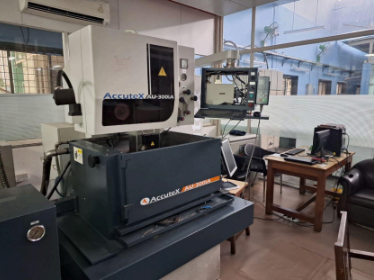
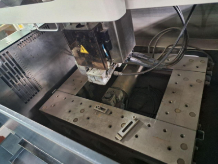
Figure (1) The image shows a Wire Electrical Discharge Machining (EDM) system, model AccuteX AU-300iA; (2) This image shows a close-up of the cutting section of a Wire EDM (Electrical Discharge Machining) machine.
- The challenge is the inefficiency and damage caused by conventional silicon wafer slicing methods, such as inner diameter saws and abrasive wire saws.
- These techniques result in high kerf loss, excessive wafer thickness, and surface damage, leading to significant material wastage, reduced productivity, and compromised wafer quality.
- This inefficiency affects the cost-effectiveness and performance in semiconductor and photovoltaic manufacturing, highlighting the need for a more efficient and less damaging slicing technology.
- Ultra-Thin Wafer Production: Capable of manufacturing wafers as thin as 100-150 μm, essential for high-efficiency photovoltaic applications.
- Reduced Kerf Loss: Achieves a 50% reduction in kerf loss compared to traditional methods.
- Contamination-Free: Avoids wire material contamination on wafer surfaces.
- Minimized Subsurface Damage: Produces wafers free from subsurface damage and amorphous layers despite using an electro-erosion process.
- Improved Surface Quality: Provides improved surface roughness from 3-5 μm to 2-3 μm .
A prototype using molybdenum wire with diameters ranging from 39 μm to 101 μm has been developed. The process involves mounting a silicon block, coupling it to the power supply, and using a MOSFET-based pulse generator to initiate the slicing. The method has been shown to reduce material wastage and improve the efficiency of photovoltaic solar cells.
The existing abrasive wire saw processes can be scaled up with multiple wires in a single setup, which is not available in the proposed solution.
8
The adoption of WEDM technology for silicon wafer slicing can lead to more efficient production processes, reducing material waste and energy consumption. This can result in lower manufacturing costs and more affordable photovoltaic products, contributing to the growth of renewable energy solutions
- Photovoltaic Cells: Manufacturing high-efficiency solar cells with thinner silicon wafers.
- Semiconductor Devices: Producing high-quality, ultra-thin silicon wafers for various semiconductor applications.
- Microelectronics: Facilitating the production of miniaturized electronic components
Geography of IP
Type of IP
2547/MUM/2013
407619