This innovation is a method for fabricating a semiconductor device, specifically a silicon carbide (SiC) power device, by depositing a stressor layer on the device. The stressor layer enhances electron mobility, increasing the ON-current and operational speed of the SiC power device. The method involves creating a drift region, p-base region, and source region through epitaxial deposition and ion implantation, followed by metallization and stressor layer deposition. This approach significantly improves the performance of SiC power devices, making them suitable for high-speed, high-power applications.
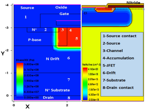
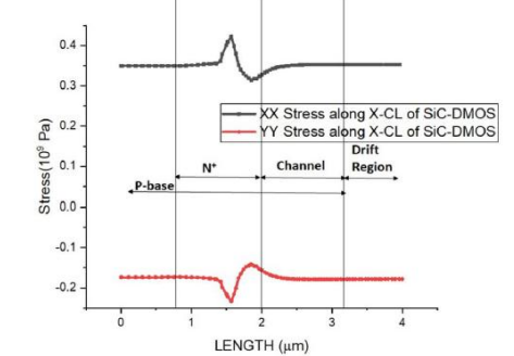
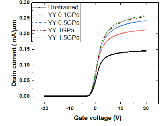
Figure (1) Schematic of the SiC power device; (2) Simulated stress profile in SiC N-channel vertical DMOSFET; (3) Drain current (ID) versus gate voltage (VG) of SiC DMOSFET showing significant improvement in ON-current
The invention addresses the challenge of enhancing the ON-current and operation speed of silicon carbide (SiC) power devices. Existing SiC devices suffer from reduced electron mobility due to traps at the SiC/SiO2 interface, leading to increased ON-resistance and lower ON-current. The proposed method introduces a stressor layer to improve electron mobility, thereby increasing the ON-current and operational speed of SiC power devices.
- Enhanced Electron Mobility: The stressor layer (e.g., Si3N4, SiO2, SiON) enhances electron mobility in the SiC power device, increasing the ON-current and operational speed.
- Process Compatibility: The method is compatible with standard semiconductor fabrication processes, making it suitable for integration into existing foundry workflows.
- Material Flexibility: The method can be applied to both SiC and gallium oxide (Ga2O3) components, providing versatility in device fabrication.
- Channel Stress: The stressor layer applies mechanical stress to the channel region, improving electron mobility and reducing ON-resistance.
- Performance Improvement: Simulations show a significant improvement in ON-current, with up to 40% enhancement under specific stress conditions.
The prototype involves a SiC layer with a drift region created by epitaxial deposition. A p-base region is formed on the drift region through masking and ion implantation, followed by the creation of an N+ source region. A SiO2 layer is deposited on the p-base and drift regions, and metallization is used to form contacts. Finally, a stressor layer (e.g., Si3N4) is deposited on the SiO2 layer, source region, and p-base region. The stressor layer is designed to apply mechanical stress to the channel region, enhancing electron mobility and improving the ON-current of the SiC power device.
Proof of Concept
3
This technology significantly enhances the performance of SiC power devices, making them more suitable for high-speed, high-power applications in electric vehicles, smart grids, and computing devices. It supports climate change commitments and energy security goals by enabling more efficient and compact power-switching circuitry, reducing energy consumption and improving overall system performance.
- Electric Vehicles: Improved power efficiency and performance
- Smart Grids: Enhanced reliability and efficiency in power distribution
- Computing Devices: Faster and more efficient power management
- Industrial Electronics: High-power, high-frequency applications
- Renewable Energy Systems: Efficient power conversion and management
- Aerospace and Defense: High-reliability, high-performance power devices
Geography of IP
Type of IP
202021021617
451441