This invention provides a method and device for creating a Gallium Nitride (GaN) bidirectional resonant tunneling diode (RTD) heterostructure. The method involves forming a quantum well layer on an upper surface of a top tunneling barrier layer, with an intermediate conducting layer between the quantum well layer and the top tunneling barrier layer. When a reverse bias is applied, the method creates a plurality of triangular barriers through which electrons in the quantum well layer tunnel sequentially, improving the device's performance in terms of negative differential conductance (NDC), peak-to-valley ratio (PVR), and reducing leakage current.
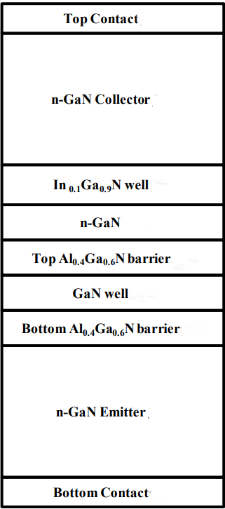
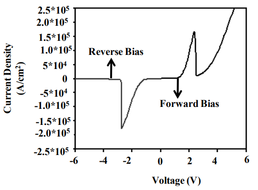
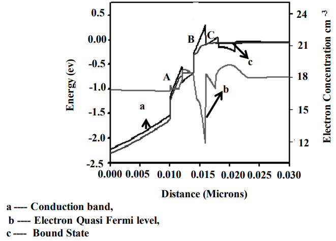
Figure (1) Schematic of the GaN bidirectional RTD heterostructure with a doped In0.1Ga0.9N layer on the collector side; (2) Current-voltage characteristics of the GaN bidirectional RTD heterostructure from -6V to +6V; (3) Band diagrams and electron concentrations at the peak and valley points under reverse bias
The invention addresses the challenge of creating a Gallium Nitride (GaN) bidirectional resonant tunneling diode (RTD) heterostructure that can operate efficiently in both forward and reverse bias. Conventional RTDs suffer from asymmetry and high leakage currents, limiting their performance in high-frequency and high-speed applications. The proposed method and device aim to enhance the performance by creating a plurality of triangular barriers through which electrons can tunnel sequentially, thereby improving parameters such as negative differential conductance (NDC), peak-to-valley ratio (PVR), and reducing leakage current.
- Quantum Well Layer Formation: The quantum well layer is formed on the upper surface of the top tunneling barrier layer, characterized by a first thickness of 3 nanometers.
- Intermediate Conducting Layer: An intermediate conducting layer is formed between the quantum well layer and the top tunneling barrier layer, characterized by a second thickness of 2 nanometers.
- Sequential Electron Tunneling: The method creates a plurality of triangular barriers through which electrons in the quantum well layer tunnel sequentially, enhancing the device's performance.
- Improved Performance Parameters: The device exhibits superior performance in terms of NDC, PVR, peak current, and valley current, especially under reverse bias.
- Reduced Leakage Current: The design significantly reduces leakage current, leading to better overall device performance.
The prototype consists of a GaN bidirectional RTD heterostructure with a bottom contact, an n-GaN emitter, a bottom barrier layer, a GaN well, a top tunneling barrier layer, a quantum well layer, an intermediate conducting layer, an n-GaN collector, and a top contact. The quantum well layer is made of In0.1Ga0.9N and is 3 nanometers thick. The intermediate conducting layer and the top tunneling barrier layer are both 2 nanometers thick. The device is tested under both forward and reverse bias, and the performance parameters such as NDC, PVR, peak current, and valley current are measured.
Demonstration and validation in lab environment
4
This technology enhances the performance of high-frequency and high-speed electronic devices, reducing power consumption and improving reliability. It enables the development of advanced computing platforms, supporting applications in terahertz frequency range and oscillators. The reduced leakage current and improved NDC and PVR make it suitable for next-generation electronics, benefiting industries such as telecommunications, computing, and defense.
- High-Frequency Applications: Suitable for terahertz frequency range devices
- Oscillators: Enhances performance in high-speed oscillators
- Telecommunications: Improves signal processing in high-speed communication systems
- Computing: Supports the development of advanced computing platforms
- Defense: Enhances the performance of radar and other defense-related electronics
- Consumer Electronics: Reduces power consumption and improves reliability in consumer devices
Geography of IP
Type of IP
3805/MUM/2014
420607