This invention is a GaN-based field-effect transistor (FET) comprising a semi-insulating SiC substrate, an AIN nucleation layer, a GaN substrate, an AlGaN barrier layer, and a gate electrode. The invention further extends to a complementary device with both n-channel and p-channel FETs, using a superlattice (SL) capping layer of InGaN/GaN pairs. This structure enables the formation of a 2-dimensional electron gas (2DEG) and a 2-dimensional hole gas (2DHG) for n-channel and p-channel transistors, respectively, facilitating high-speed and efficient digital computations on the rugged wide-bandgap (GaN) platform.
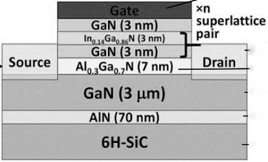
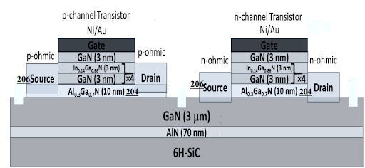
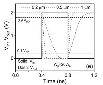
Figure (1) Schematic of the complete structure with the SL capping layer of the GaN-based E-mode transistor; (2) Schematic of the complementary GaN-based field effect transistor device; (3) Simulated propagation delay of the inverter for various channel lengths
The invention addresses the challenge of realizing monolithic complementary n-channel and p-channel GaN-based field-effect transistors (FETs) for efficient digital computations. Traditional GaN technology has lacked reliable p-channel FETs, leading to the use of heterogeneous integration with Si-based CMOS, which is less efficient. The invention introduces a superlattice (SL) capping layer of InGaN/GaN pairs on an AlGaN barrier layer to form complementary E-mode transistors, thereby overcoming the limitations of conventional GaN technology.
- Complementary Transistor Structure: The invention utilizes a superlattice (SL) capping layer of InGaN/GaN pairs to create complementary E-mode transistors, addressing the lack of reliable p-channel FETs in GaN technology.
- Enhanced Field-Effect Transistors: The SL pairs move the band-edges up, creating a natural quantum well for holes and facilitating the formation of 2DHG, while depleting the 2DEG at equilibrium.
- High Performance and Low Delay: The complementary devices exhibit a propagation delay of ~10-15 ps, indicating that logic operations can be performed at very high speeds compared to conventional semiconductors.
- Compatibility with Existing Processes: The invention uses well-established epitaxial growth techniques and metal deposition methods, making it suitable for integration into existing foundry workflows.
- Reduced Parasitic Effects: The complementary behavior ensures that the active channels do not see the complementary channel, even though they are aligned vertically, thus avoiding parasitic delay.
The prototype consists of a semi-insulating SiC substrate with an AIN nucleation layer, a GaN substrate, and an AlGaN barrier layer. The superlattice (SL) capping layer of InGaN/GaN pairs is deposited on the AlGaN barrier layer. The n-channel and p-channel FETs are formed using appropriate ohmic contacts. The gate electrode is deposited on the final GaN layer. The device is fabricated using standard epitaxial growth techniques and metal deposition methods. The 2DEG and 2DHG densities are controlled by the number of SL pairs and the gate bias, ensuring efficient and reliable operation.
Proof of concept
3
The invention enables high-speed and efficient digital computations, reduces the memory-compute bottleneck in large-scale data processing tasks, and supports the development of scalable, low-power electronic devices essential for edge computing and embedded systems. It advances indigenous microelectronics research and development capabilities, promoting technological sovereignty and innovation.
- Digital Logic Circuits: High-speed, low-power digital logic gates
- Power Electronics: Efficient power switching and conditioning
- RF Applications: High-frequency power amplifiers and transmitters
- Edge AI and IoT Devices: Scalable, low-power computing for edge devices
- Data Centers: High-performance computing (HPC) and data processing
- Neuromorphic Computing: Advanced computing architectures and accelerators
Geography of IP
Type of IP
202121016813
409302