This invention presents a technology balancing transformer (BALUN), Low Noise Amplifier (LNA) Mixer (BLIXER) architecture for wideband radio receivers. It combines the functions of a BALUN LNA, and mixer into a single, compact, and power-efficient circuit. The BLIXER uses folding techniques and CMOS inverter-based switching to address voltage headroom limitations and reduce flicker noise. By enabling in-phase and quadrature-phase signal processing, it supports high-frequency applications (up to 6 GHz) while achieving improved gain, linearity, and reduced component count in radio frequency (RF) front-end design.
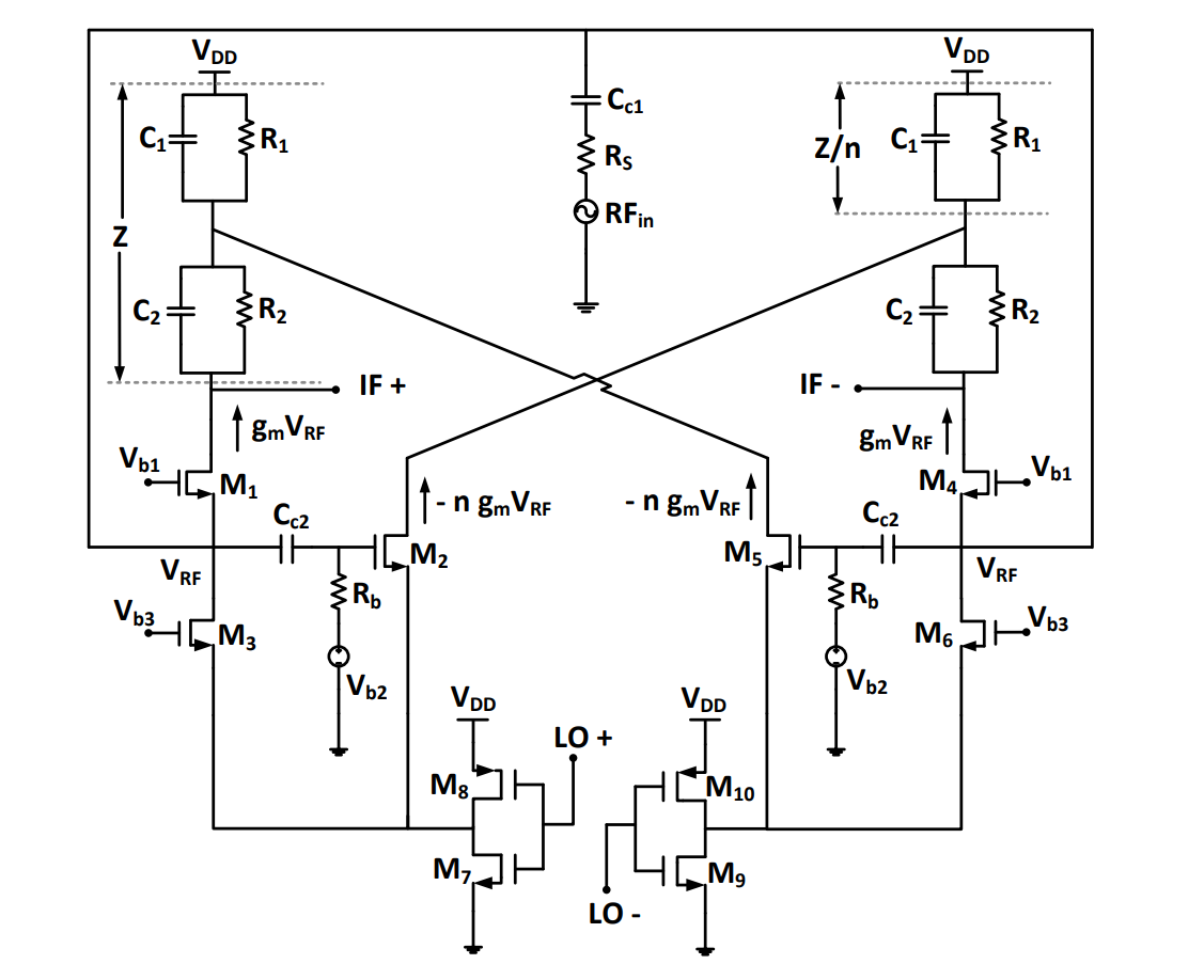
Figure 1. Switched transconductor BLIXER topology with CMOS inverter as switches
Wideband receivers used in modern communication systems suffer from high complexity, power consumption, and cost due to the need for external SAW filters and multiple discrete components. Traditional mixer-LNA configurations face challenges such as voltage headroom issues, poor noise performance, and large chip area. There is a strong need for a compact, low-power, integrated RF front-end that can efficiently support wide frequency bands without external filtering components.
- Integrated RF Front-End Architecture: The invention BLIXER reduces the need for bulky external components in wideband receivers like SAW filters, separate baluns, and discrete mixers and amplifiers, leading to higher cost, complexity, and power consumption.
- Folding-Based Current Buffering: A folding technique is introduced in the current buffer stages, allowing the conversion of NMOS-based buffers to PMOS buffers. This reduces headroom issues and enables operation under low supply voltages.
- Enhanced Gain through Current Mirroring: The design includes a current mirroring approach for gain enhancement, which increases the signal current before the mixing stage, improving the receiver’s sensitivity.
- Switching Efficiency with CMOS Inverters: The BLIXER uses CMOS inverter-based switching for the mixer stage, allowing low-ohmic, fast switching with minimal voltage overhead, which is crucial for wideband operation.
- Noise and Linearity Optimization: The proposed configuration reduces flicker noise using PMOS switches and enables better linearity by minimizing the number of RF-transmitting transistors in the signal path.
The proposed BLIXER was implemented using 65 nm CMOS technology and designed to operate at a supply voltage of 1.2 V. Simulation results demonstrate a high conversion gain of up to 38 dB with a -3 dB bandwidth reaching 6 GHz, making it suitable for wideband applications. The noise performance is competitive, with a noise figure of approximately 6.5 dB at a 100 MHz intermediate frequency (IF). Additionally, the design achieves a third-order input intercept point (IIP3) of -19 dBm, indicating good linearity. The BLIXER supports differential outputs and can operate in I/Q topology using 25% duty cycle clocks, allowing precise in-phase and quadrature-phase signal generation required for modern RF receivers.
The BLIXER design has been validated through circuit simulations using 65 nm CMOS technology. Key parameters like gain, noise figure, and linearity have been analyzed. The technology is currently at TRL 4, with successful simulation-based demonstration in a lab environment.
4
The proposed BLIXER technology can significantly contribute to making compact, low-cost, and high-performance wireless communication devices more accessible. It is particularly useful in enabling the next generation of 5G, software-defined radios, and ultra-wideband (UWB) communication systems. By reducing power consumption and chip area, it supports the development of more affordable and energy-efficient mobile and IoT devices, contributing to digital connectivity in remote or underserved areas.
- Wireless communication systems (4G, 5G, Wi-Fi, UWB)
- Software-Defined Radios (SDRs)
- RF front-end modules in smartphones and IoT devices
- Aerospace and defense communication systems
- Semiconductor and chip design industries
Geography of IP
Type of IP
201921010070
560007