An adaptive linear equalizer is presented for use in high-speed data receivers to recover distorted signals caused by inter-symbol interference (ISI) and high-frequency loss during transmission. The equalizer incorporates a frequency detector that compares the received data's frequency components with a reference, generating a control voltage. This voltage tunes a hybrid active filter's low-pass and high-pass filters to balance their outputs. A charge pump uses the spectral difference between these outputs to further refine the control voltage, which then drives a boost circuit that amplifies the appropriate frequency components of the received data. The design is inductor-less, power-efficient, compact, and adaptable across a wide data rate range (4 Gbps to 14 Gbps), making it suitable for high-speed communication applications in modern integrated circuits.
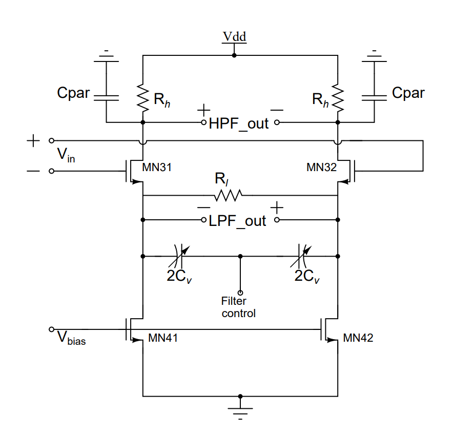
Figure 1. Proposed hybrid active filter
Traditional adaptive linear equalizers suffer from limited adaptability due to fixed filter components, increased power consumption due to slicer use, and performance degradation under process variations. This leads to inefficient equalization of distorted signals at high data rates, particularly in the presence of significant ISI (Inter Symbol Interference) and high-frequency losses in modern communication systems.
- Adaptive Frequency Detection: The invention uses a frequency detector to generate a control voltage based on the difference between a reference frequency and the frequency content of the incoming signal.
- Tunable Hybrid Active Filter: The cut-off frequencies of the low-pass and high-pass filters are dynamically tuned using variable capacitors, allowing equalization to adapt across a wide data rate range (4–14 Gbps).
- Spectrum Balancing Using Power Comparison: By comparing the power of the HPF and LPF outputs, the design ensures accurate adjustment without the need for slicers, reducing power overhead.
- Inductor-less High-Frequency Boost Circuit: The boost circuit amplifies desired frequency components without using inductors, resulting in a compact, CMOS-compatible implementation.
- Process Variation Compensation: The use of voltage-controlled capacitance tuning helps in mitigating the effects of manufacturing variations, enabling robust equalization performance.
- Compact and Low-Power Design: The architecture uses fewer passive elements, achieves a small core area (350 µm × 130 µm), and consumes only 25 mW (1.8 mW/Gbps) in 65 nm CMOS technology.
The prototype of the adaptive linear equalizer was implemented in 65 nm CMOS mixed-mode process technology. The system includes a receiver-integrated adaptive equalizer capable of operating over 4 Gbps to 14 Gbps. Post-layout simulations were carried out under practical conditions, including a differential signal swing of 400 mVpp, a random jitter of 35%, and input from a non-ideal package model. The equalizer was validated against channel losses up to 12 dB at 14 Gbps. Simulations included eye diagrams that showed a fully closed eye at input and a significantly opened eye at the output. A 150 µF capacitive load emulating driver input was used to verify output strength, demonstrating successful signal recovery and performance under real-world constraints.
A post-layout simulated adaptive equalizer has been developed in 65 nm CMOS, achieving data rates up to 14 Gbps with 12 dB channel loss compensation, while consuming 25 mW power. It features a tunable hybrid filter and boost circuit for high-speed, low-power signal recovery.
4
This innovation improves reliability and speed of high-bandwidth digital communication systems used in consumer electronics, telecom, and computing infrastructure. Contributes to efficient, low-power data transmission in future chipsets and network devices.
- High-speed serial communication (e.g., SerDes)
- Ethernet and data center hardware
- Integrated circuit (IC) design for communication chips
- Telecom and networking systems
- Signal integrity solutions in chip design
- Consumer electronics requiring high-speed data transfer
Geography of IP
Type of IP
4165/MUM/2014
386017