This invention discloses a tunable reference voltage generating circuit that achieves high precision and stability across variations in process, voltage, and temperature (PVT). The circuit integrates a tunable current generator to control bias currents for both Proportional To Absolute Temperature (PTAT) and Complementary To Absolute Temperature (CTAT) voltage generators. These modified voltages are then averaged using a switched capacitor circuit to produce a stable output reference voltage. An on-chip 8-bit shift register allows digital tuning without requiring external trimming or calibration circuits. The design eliminates resistors by using sub-threshold MOSFET operation, resulting in a compact, energy-efficient solution. With excellent Power Supply Noise Rejection (PSNR > 80 dB), low power consumption (as low as 120 nW), and minimal chip area (0.023 mm²), this reference generator is ideally suited for use in analog and mixed-signal integrated circuits, energy harvesting systems, and low-power sensor interfaces.
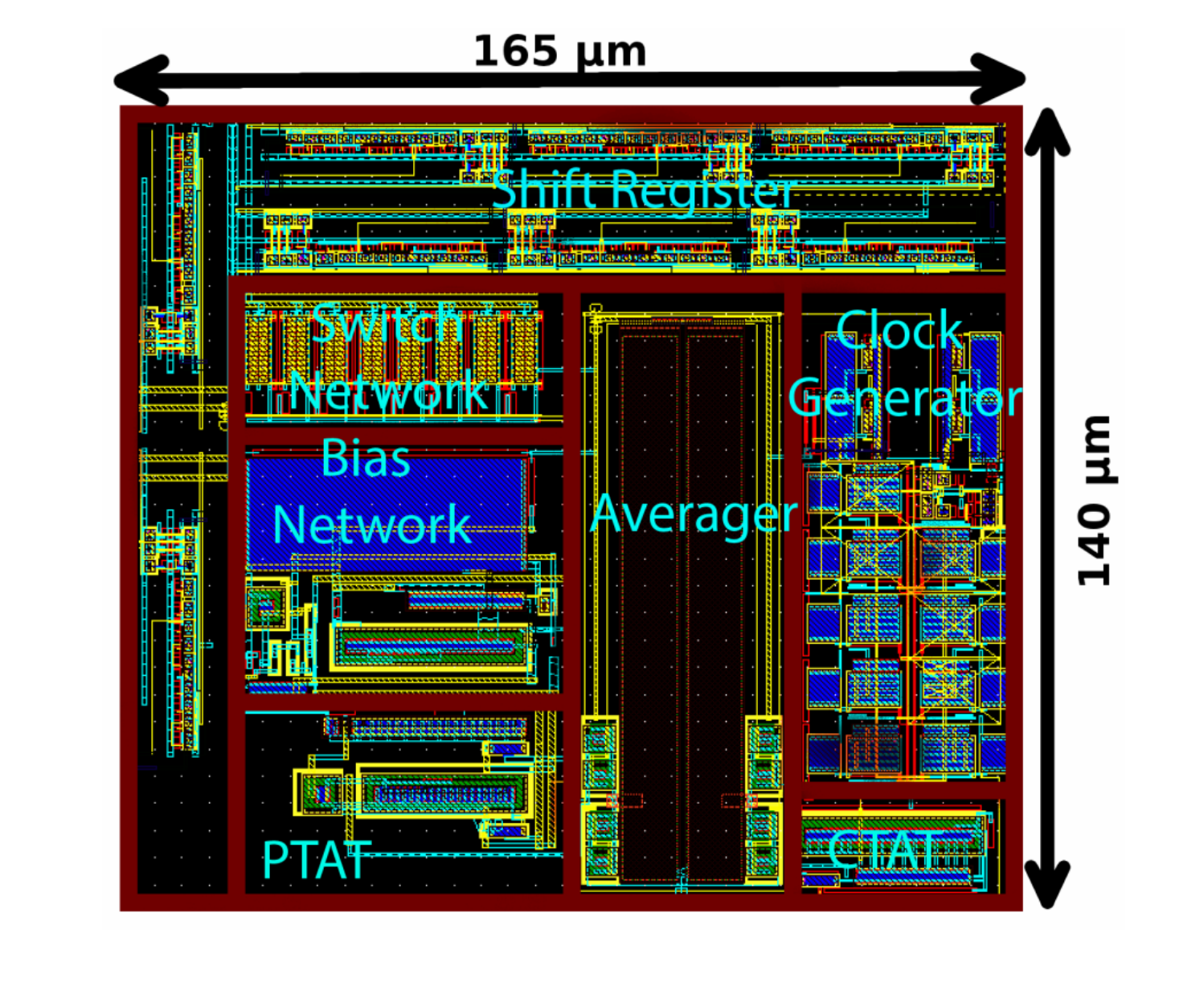
Figure 1. Complete layout of the design
Analog and mixed-signal integrated circuits (ICs) like ADCs, DACs, and memory modules require stable reference voltages. Existing bandgap reference generators often show temperature and process sensitivity or occupy a large silicon area due to large resistors. There is a need for a compact, tunable, and process-voltage-temperature (PVT) invariant reference voltage generator with low power consumption and better power supply noise rejection (PSNR).
- Tunable Biasing for PTAT and CTAT Generators: The reference voltage generating circuit employs a tunable bias current circuit to fine-tune both the Proportional To Absolute Temperature (PTAT) and Complementary To Absolute Temperature (CTAT) voltage generators, enabling precise control of the reference voltage.
- Resistor-less Compact Design: The design eliminates the need for on-chip resistors by using MOSFETs operating in the sub-threshold region, which significantly reduces silicon area and supports efficient integration in compact IC layouts.
- Digital Control Using Shift Register: The circuit includes an 8-bit digital shift register that facilitates programmable tuning by selectively activating one of eight transistors with different aspect ratios, thus enabling adaptable and precise voltage control post-fabrication.
- Switched Capacitor-Based Voltage Averaging: The system utilizes a switched capacitor network to average the PTAT and CTAT voltages, producing a stable and PVT invariant reference voltage without requiring analog filtering components.
- High Power Supply Noise Rejection (PSNR) and Line Regulation: The design achieves high PSNR exceeding 80 dB with a 1 pF filter capacitor and maintains robust line regulation of 0.18%/V, while ensuring that temperature sensitivity and overall voltage stability are not compromised.
- Ultra-Low Power and Area Efficient Implementation: The reference generator occupies only 0.023 mm² of chip area and consumes minimal power—120 nW at 0.8 V and 300 nW at 1.8 V—making it highly suitable for low-power, battery-operated, and energy-harvesting electronic systems.
The prototype of the tunable reference voltage generating circuit was implemented using the UMC 180 nm CMOS process. The design integrates key elements including PTAT and CTAT voltage generators, a supply-independent tunable current source, an 8-bit shift register for digital control, and a switched capacitor-based averaging circuit. The reference voltage output is tunable around 230 mV, with minimal variation (±0.28%) across different process corners. The circuit operates reliably across a wide temperature range of -25°C to 100°C and supports supply voltages ranging from 0.8 V to 1.8 V. Post-layout simulations validated the design’s robustness, showing that the output voltage maintains stability within ±2.1% across 1000 Monte Carlo runs, a variation range that is effectively compensated through the built-in tuning mechanism.
The circuit design has been developed, validated through circuit simulations and tested in lab conditions.
3
The tunable reference generator enables more precise and energy-efficient analog and mixed-signal ICs. Applications in low-power electronics, environmental sensors, healthcare devices, and next-generation communication systems benefit from improved stability and reduced manufacturing variability.
- Analog and Mixed-Signal IC Design
- ADC/DAC modules
- Energy Harvesting Systems
- Sensor Interfaces
- IoT Devices
- Precision Instrumentation
Geography of IP
Type of IP
2464/MUM/2015
374571