The invention relates to a hysteretic controlled DC-DC buck converter capable of operating across the full range of lithium-ion battery voltages. It uses a stacked NMOS/PMOS configuration powered by an internal 2.4 V regulated supply, a high-speed hysteretic comparator for stable switching, and a dual-mode control system enabling efficient operation in both pulse width modulation (PWM) and pulse frequency modulation (PFM) regimes. The design incorporates level-shifting drivers, scalable inverters, and bias regulators for robust performance over process, voltage, and temperature variations.
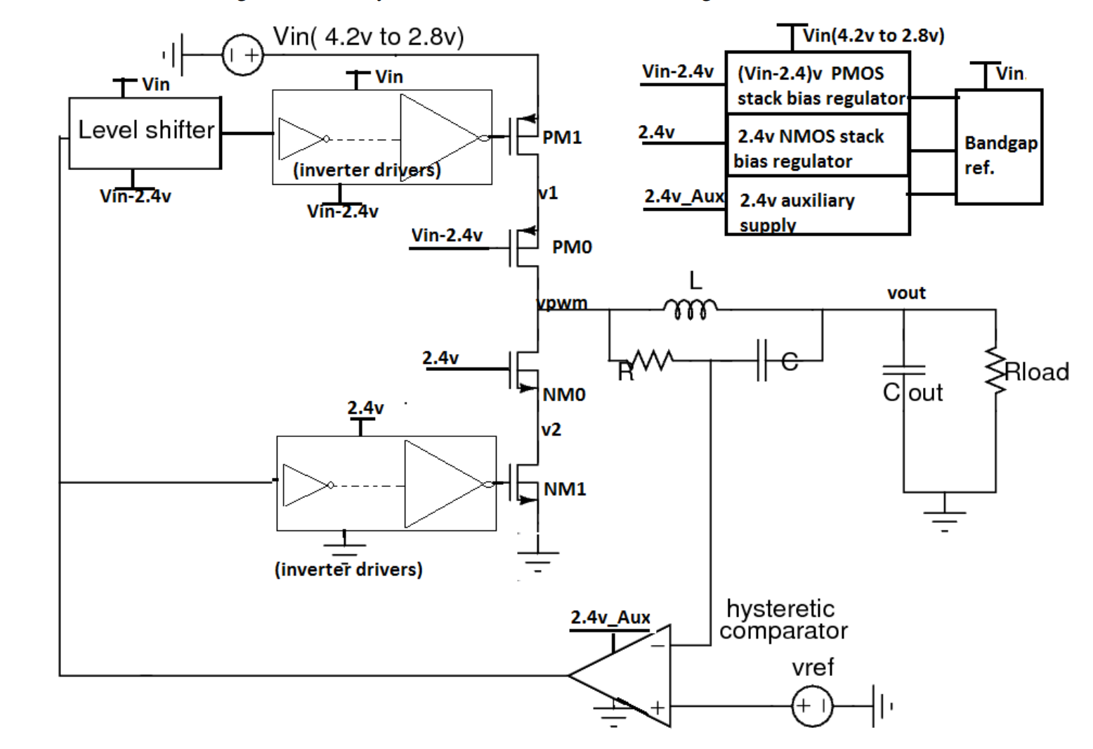
Figure 1. Hysteretic PWM buck converter with transistor stacking using ideal drivers
Conventional buck converters face challenges in power efficiency, noise immunity, and integration when designed for lithium-ion battery ranges. Generating a compact, robust, and low-ripple power supply across wide input conditions with process and temperature stability is a critical need in battery-powered systems.
- Stacked Transistor Architecture: The converter employs stacked PMOS and NMOS devices optimized for wide battery voltage ranges and minimal gate stress through regulated biasing.
- Hysteretic Comparator: A high-speed comparator with a 28 mV hysteresis window ensures noise immunity and clean switching thresholds during low- and high-current transitions.
- Level-Shifting Drivers: The level shifter feeds progressively scaled inverter chains that deliver sharp transitions to the power switches, maintaining efficiency and timing precision.
- Internal Power Management Unit: Integrated bandgap references and regulators provide a 2.4 V auxiliary supply, enabling consistent gate control and biasing across operating modes.
- Mode Adaptability: The converter supports both pulse width modulation (PWM) and pulse frequency modulation (PFM) modes for continuous and discontinuous conduction, respectively, with automatic transition controlled via digital MUX and external signals.
The prototype design consists of a comparator-driven control loop with a hysteresis of 28 mV, stacked transistor power switches, a bandgap reference for bias generation, and digitally controlled MUX for PWM/PFM mode switching. Internal power management ensures 2.4 V regulated control signals. The circuit is optimized for operation over the lithium-ion voltage range and verified through extensive simulations.
A post-layout simulated converter in 90 nm CMOS has been developed, delivering 0.8–1.8 V output from a 2.8–4.2 V Li-ion input with up to 92.5% efficiency. It supports PWM–PFM switching, operates from 100 pA to 200 mA, and is optimized for portable electronics.
3
The converter reduces energy waste and enhances battery life in consumer electronics, wearables, and IoT applications. Offers scalable voltage regulation with robust performance, facilitating compact power management in future electronic systems.
- Wearable electronics
- Internet of Things (IoT)
- Smart sensors
- Lithium-ion battery-powered devices
- Mobile and embedded systems
Geography of IP
Type of IP
3257/MUM/2012
371616