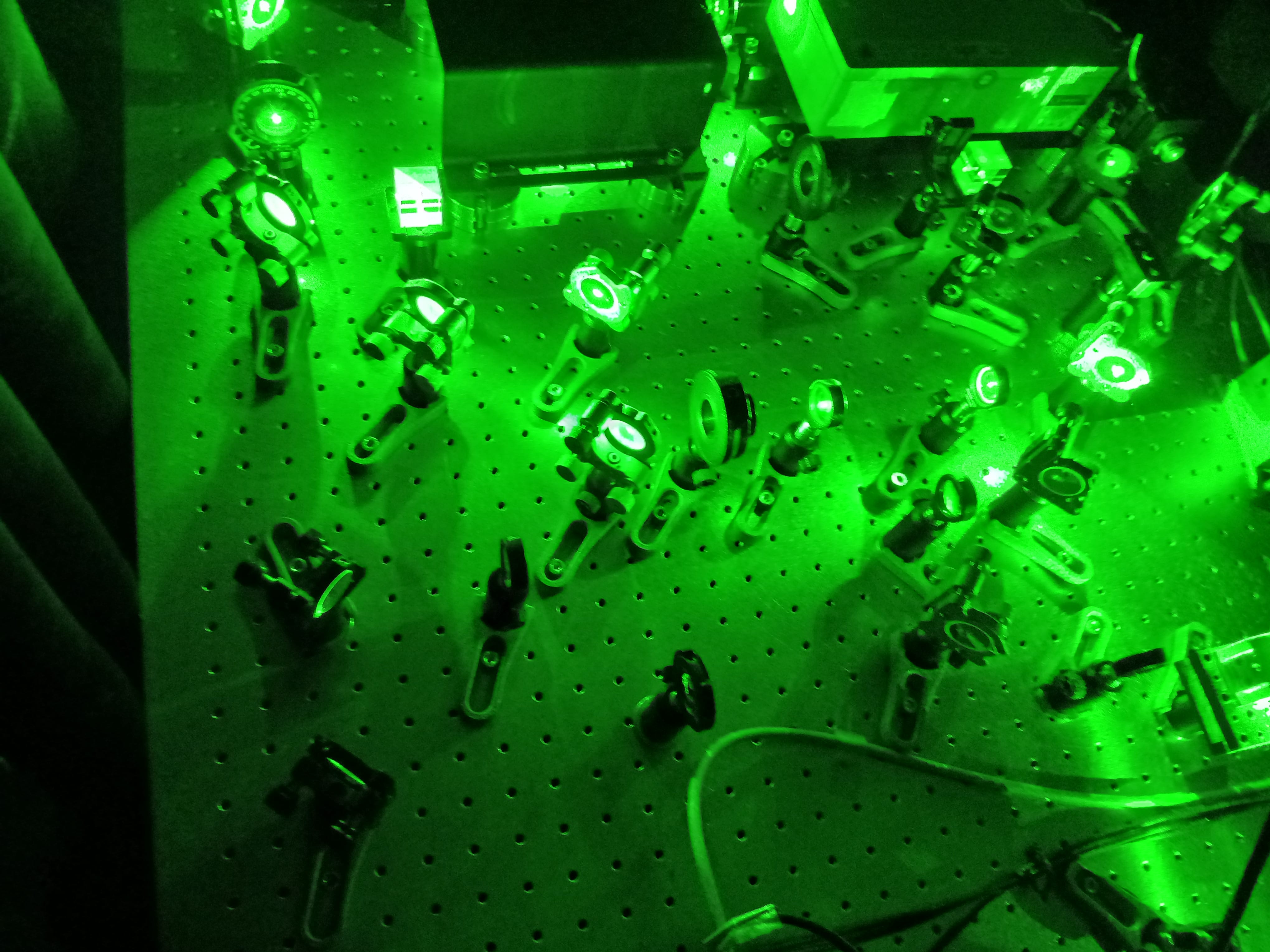
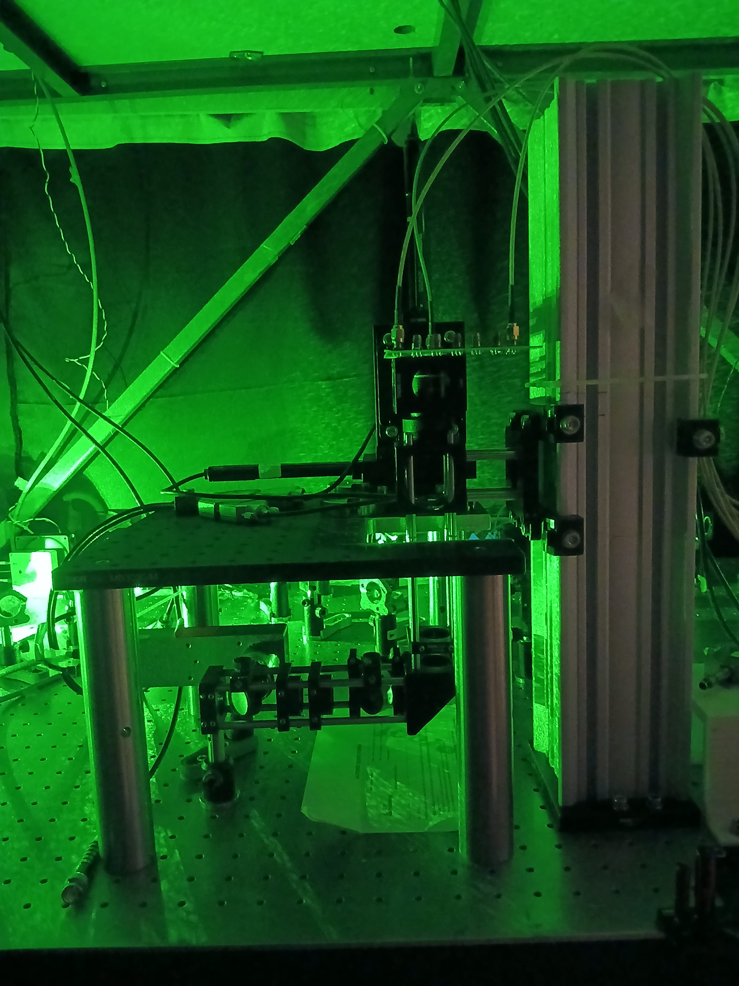
This is an innovative device for visualizing dynamic magnetic fields using diamonds with special defects called nitrogen-vacancy (NV) centers. The device includes a diamond with NV centers, a laser to make these centers glow, and a microwave system to interact with them. It also has a microscope to capture high-speed, wide-area images and a detector to create detailed maps of magnetic fields. The device can operate in two modes: one that measures magnetic fields at a single point and another that measures it across a larger area. This allows for dynamic and detailed imaging of magnetic fields.
Micro-Tesla sensitivity widefield magnetic field imaging has been performed in the past using NV defects in diamond. While the previous methods allow probing microscale magnetic field information, the acquisition time of a single magnetic field image ranges from few to several minutes. Due to this limitation, the NV based widefield magnetic imaging is limited to static fields and imaging of time dependent fields is not possible.
- The apparatus for magnetic field imaging utilizing nitrogen-vacancy (NV) defect centers in diamonds is designed to achieve high sensitivity and resolution.
- The capabilities of the widefield NV based magnetometers have been extended to image widefield 2D magnetic fields varying on a few milliseconds timescale, which would allow measurements of time-dependent 2D magnetic field microscopy. This is achieved by using lock-in technology to enhance signal detection.
- The optical radiation detector operates in two modes: Single Photodiode Diamond NV Magnetometry (SP) Mode and Wide Field Per Pixel Lock-In Diamond NV Magnetometry (WM) Mode. The SP mode uses a single photodiode for bulk single-point magnetometry, while the WM mode employs a 2D array of optical detectors to perform high-speed, wide-field imaging.
- The imaging method leverages lock-in technology to enhance signal detection. In WM mode, a 2D array of optical detectors performs frequency-locked light detection, allowing for high-speed magnetic field imaging. By synchronizing applied microwave frequencies with internal frames of a lock-in camera, the system captures in-phase (I) and quadrature (Q) values for each pixel. These values are averaged over multiple cycles to produce a pair of 2D images representing the magnetic field information. This approach significantly improves the signal-to-noise ratio, enabling the detection of weak magnetic fields with high sensitivity.
The apparatus achieves mean magnetic field sensitivities of 22.18 μT/√Hz per pixel in WM mode and 11.6 nT/√Hz in SP mode.
Additionally, it can perform wide-field magnetometry for time-dependent bulk magnetic fields varying at 1-10 Hz, with image acquisition frame rates ranging from 40-200 Hz.
The apparatus exhibits high sensitivity, achieving mean magnetic field sensitivities of 22.18 μT/√Hz per pixel in Wide Mode (WM) and 11.6 nT/√Hz in Super-Precision Mode (SP). Additionally, it can perform wide-field magnetometry for time-dependent bulk magnetic fields varying between 1 and 10 Hz, with image acquisition frame rates ranging from 40 to 200 frames per second.
It also demonstrates the capability to precisely measure micro-scale AC magnetic fields using NV centers in diamond within a widefield configuration to successfully detect the resulting stray fields, corresponding to changes of approximately 1 femtojoule per Tesla in magnetic moment.
4
- Dynamic widefield imaging can be useful for probing physics of thin 2D materials and time-dependent magnetic fields in biological tissue like neurons and iron nanoparticles loaded biological cells.
- It is also useful in detecting faults in semiconductor chips, and analysing effects of different oxide layers in MOSFETs.
- It can also be used to detect micron-sized magnetic particles due to highly sensitive AC susceptibility measurement capabilities. Hence, this invention can help detect magnetic fields of any thin material in a highly sensitive and non-invasive manner.
- Biomedical: Dynamic widefield imaging can be useful for probing physics of thin 2D materials and time-dependent magnetic fields in biological tissue like neurons and iron nanoparticles loaded biological cells.
- Semiconductors, electronics: It is also useful in detecting faults in semiconductor chips, and analysing effects of different oxide layers in MOSFETs. It can also be used to detect micron-sized magnetic particles due to highly sensitive AC susceptibility measurement capabilities.
Geography of IP
Type of IP
202121010532
408534


