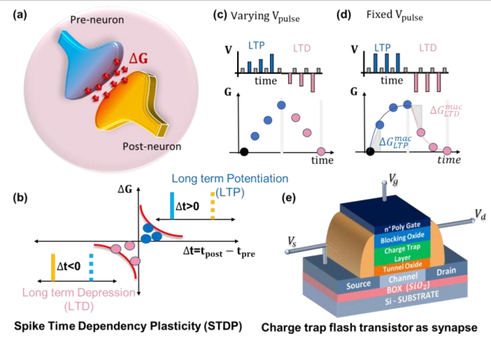
The proposed technology involves a synapse based on highly manufacturable Charge Trap Flash (CTF) Memory on Silicon-On-Insulator (SOI) technology. It demonstrates gradual symmetric Long-Term Potentiation (LTP) and Long-Term Depression (LTD) with arbitrarily tunable states, making it suitable for neuromorphic computing applications.
Figure (1a) A synapse in a human body between neurons; (1b) A graph plot illustrating synaptic conductance change (ΔG) with respect to spike time difference (Δ𝑡); (1c) Illustrates 𝐺 changes with varying Vpulse; (1d) Illustrates 𝐺 changes with fixed Vpulse; (1e) Proposed synapse implemented in a Charge Trap Flash (CTF)
The key issue addressed is the need for an efficient and reliable synaptic device that can mimic biological synapses for neuromorphic computing, with low energy consumption, CMOS compatibility, and technological maturity.
- Gradual symmetric LTP and LTD demonstrated
- Tunable number of states (101 to 104) by pulse characteristics
- Spike-Timing Dependent Plasticity (STDP) demonstrated by FN tunneling
- Synaptic unit cell size of 30F²
- Endurance of more than 109 LTP/LTD cycles
- Energy-efficient with <660 aJ per essential energy spike
The synaptic device is implemented on an SOI substrate with a 1F2D configuration. The prototype includes back-to-back Zener and standard pn diodes to block undesirable current during operation, ensuring efficient performance in a cross-bar array network.
The technology is implemented with a single cell Charge Trap Flash (CTF) memory for ultra-low energy synapses (<2fJ). These synaptic cells effectively represent tunable and symmetric learning capabilities, demonstrating their utility in Spiking Neural Networks (SNN) and Deep Neural Networks (DNN) algorithms for neuromorphic computing.
3
The technology enables the development of efficient and scalable neuromorphic systems, contributing to advancements in AI and machine learning. This can lead to more energy-efficient computing systems and potentially transform various sectors by providing more intelligent and adaptive technologies.
The primary application of this technology is in neuromorphic computing systems, where it can be used to build large-scale neural networks that mimic the human brain's learning and energy efficiency. It is particularly suited for real-time learning applications and advanced AI system.
Geography of IP
Type of IP
201921006118
531548

