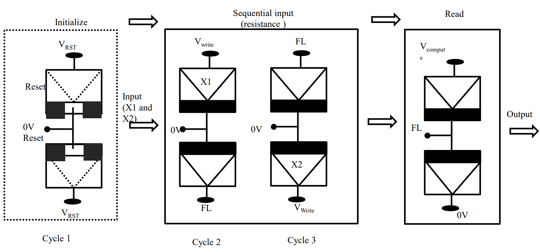
The patent describes a method for fabricating a three-terminal resistive random-access memory (3T-RRAM) device. This device aims to improve in-memory computing by integrating logical operations within the memory, addressing the von Neumann bottleneck, which limits conventional computing performance due to data transfer inefficiencies between the processor and memory.
The von Neumann bottleneck in conventional computing creates inefficiencies in handling data-intensive tasks, particularly in AI applications, due to high communication overhead between the processing unit and memory unit. Existing RRAM solutions require multiple cycles and multiple devices, leading to inefficiencies in energy and speed.
- This technology includes three contacts that serve as both input and output terminals.
- The fabrication involves multiple layers, including silicon, silicon dioxide, titanium, platinum, zirconium dioxide, and PCMO.
- There is a single write cycle for logical operations with voltage input and resistance output.
- It reduces communication overhead between processor and memory.
- It increases energy efficiency and reduces latency in data-intensive tasks.
- It simplifies device architecture by reducing the number of required components and operations.
- A multi-layered structure with specific materials (Si, SiO2, Ti, Pt, ZrO2, PCMO, W).
- Uses buffered hydrogen fluoride (BHF) for etching to create the necessary patterns.
- The device demonstrates a 3T-RRAM configuration that integrates both storage and computational capabilities.
The functionality of handling logic operation in a 3-terminal memory device has been demonstrated. The logic operation requires a single input and a single compute cycle. The optimization of the material composition of the memory device for low-power in-memory computing is ongoing.
4
This technology enhances the performance and efficiency of AI and data-intensive applications, potentially accelerating advancements in these fields. It reduces energy consumption in data centers, contributing to greener technology solutions. It improves the capabilities of consumer electronics and IoT devices, leading to better user experiences and more advanced functionalities.
- Artificial Intelligence (AI) and machine learning tasks
- Data centers and cloud computing
- High-performance computing (HPC)
- Real-time data analytics
- Consumer electronics embedded systems
- IoT (Internet of Things) devices requiring efficient data processing and storage
Geography of IP
Type of IP
202021018935
496652

