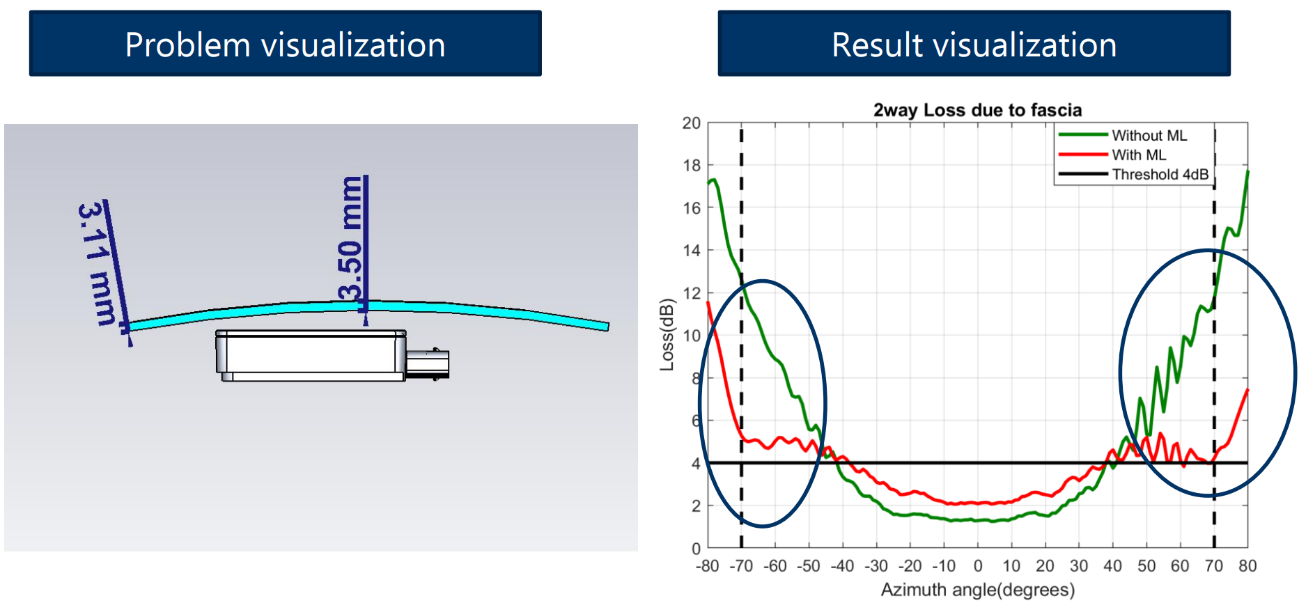
The invention pertains to a method and electronic device designed to create a non-uniformly thick matching layer for 3D components in vehicles, such as bumpers, that house radar modules. This matching layer aims to minimize the reflection and losses of microwaves caused by the bumper's curvature and materials. The method involves using a binomial matching layer technique to design this layer based on the thickness and dielectric properties of the 3D component.
Integration of automotive radar modules behind vehicle bumpers introduces losses due to the bumper's curvature, dielectric properties, and reflective paint materials. These losses distort the radar module's radiation patterns and reduce field intensity, compromising the radar's performance.
- This innovation reduces microwave reflections and integration losses for radar modules placed behind vehicle bumpers.
- It enhances the performance of radar modules by maintaining the integrity of their radiation patterns.
- It adapts to the non-uniform thickness of the 3D component, providing a tailored solution that addresses specific design and material challenges.
Technical Features:
- Generation of a non-uniformly thick matching layer based on the 3D component's thickness and dielectric constant
- Use of a binomial matching layer technique to optimize the matching layer's effectiveness
- Consideration of parameters such as impedance, load, and free space impedance
- Representation of the 3D component surface using triangles in a 3D Cartesian Coordinate System for precise modeling
The prototype involves an electronic device equipped with a processor, memory, radar module, and a 3D layer designing tool. This device would receive the design of a non-uniformly thick 3D component, determine its thickness at various locations, and generate a corresponding binomial matching layer to optimize radar performance.
Early prototype development and validation in relevant environment has been completed.
5
This innovation enhances vehicle safety by improving the reliability and accuracy of radar-based detection systems. It reduces the risk of accidents by ensuring better functionality of radar modules in various driving conditions.
- Automotive industry - particularly in the design and manufacturing of vehicle bumpers and radar modules
- Advanced driver-assistance systems (ADAS) that rely on radar for object detection and relative positioning
- Other industries requiring radar modules
Geography of IP
Type of IP
202241056351
530089

