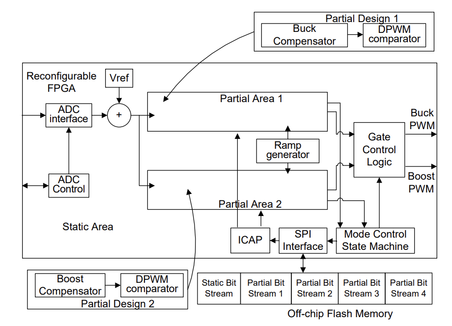
This invention presents a new method for controlling a non-inverting buck-boost converter using an FPGA with dynamic reconfiguration. Unlike traditional converters that use a single controller for both buck and boost modes, this approach uses separate controllers optimized for each mode. The FPGA adjusts in real-time: configuring only the necessary circuits for the current mode (buck, boost, or both). This not only improves efficiency but also reduces power consumption by up to 48%. The system ensures smooth transitions between modes, maintaining stable output voltage even during changes in input voltage or load. Overall, it represents a significant advancement in power electronics, offering better performance and energy savings.
Traditional non-inverting buck-boost converters face challenges with using a single controller for both buck and boost modes, which limits optimization and increases resource consumption in FPGAs. This leads to inefficiencies in power management and higher heat generation.
- Dynamic reconfiguration: The invention enables FPGA to switch between buck, boost, and combination modes on-the-fly, optimizing resource allocation and enhancing flexibility in power management.
- Resource efficiency: It reduces FPGA resource usage by up to 48%, minimizing hardware footprint and lowering costs associated with design and implementation.
- Seamless mode transitions: It facilitates smooth transitions between different operational modes, ensuring continuous and stable performance under varying load and input conditions.
- Enhanced voltage regulation: It improves output voltage stability and accuracy, crucial for applications requiring consistent power supply across dynamic operating environments.
- Power consumption optimization: The overall power consumption of the system is lowered by efficiently utilizing FPGA resources based on current operational requirements, contributing to energy savings.
- Improved thermal management: It mitigates heat generation within the FPGA, enhancing reliability and lifespan of electronic components while maintaining optimal operating temperatures.
- Scalability and versatility: It provides scalability for future enhancements and versatility to adapt to different application requirements without significant hardware modifications, ensuring long-term usability and adaptability.
The technology was demonstrated in lab environment using Run-Time Partial Reconfiguration of Xilinx Spartan-6 FPGA along with other associated components of buck-boost circuit.
Further development/prototype manufacturing is not carried out. However, the run-time partial reconfiguration of FPGA remains a relevant technology in various applications.
4
This innovation enhances energy efficiency, reducing overall power consumption. It improves reliability and lifespan of electronic devices and supports sustainable technology development. It enables stable power supply in various environments. It facilitates cost-effective design solutions and contributes to reduction of electronic waste.
Power electronics, renewable energy systems, automotive electronics, industrial automation, consumer electronics, telecommunications, portable devices, smart grids
Geography of IP
Type of IP
515/MUM/2013
428237

