The researchers have developed a novel method of using silicon nitride to enhance the efficiency of photonic elements, promising faster, more secure, and energy-efficient technologies for communication and information processing.
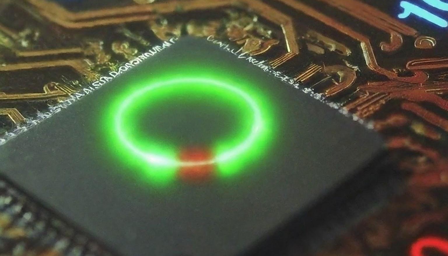
Image: Generated by Gemini AI
Photonic technology manipulates photons (particles of light) in a similar way as electronic devices handle electrons. This emerging field promises faster, more secure and energy-efficient technologies. In a recent study, researchers from the Indian Institute of Technology Bombay (IIT Bombay) and Tata Institute of Fundamental Research (TIFR) have developed an innovative method using silicon nitride (SiN) to enhance the efficiency of photonic elements, which are the future of communication and information processing technology.
Typically, creating photonic elements involves complex fabrication and encounters certain challenges, such as poor stability and optical losses leading to low-efficiency performance. One of the main complications arises because the light source (emitters) and photonic elements consist of different materials. This poses a challenge known as poor "coupling efficiency" which means that the light from the source is not perfectly guided into the photonic element, leading to losses and degraded performance.
To address this, researchers have been exploring ways to use the same material for both the emitters and the photonic elements, a concept known as "monolithic integration". In this study, the team of researchers turned to silicon nitride (SiN), a material that has shown potential as a good single-photon emitter at room temperature. Silicon nitride has the added benefit of being compatible with current widespread semiconductor production techniques, known as CMOS technology.
Prof Anshuman Kumar Srivastava from IIT Bombay explains, “Silicon nitride stands as a pioneering material in the realm of nanophotonics, boasting well-established prowess in the construction of integrated photonics circuits. The prominence of this work stems from the innate emitters inherent within SiN.” By managing the manipulation and enhancement of these intrinsic emissions, scientists can unlock a vast array of solutions for integrated photonics applications. “This can help harness existing capabilities of SiN and pioneer novel avenues in photonics integration, promising groundbreaking advancements in optical technologies,” adds Prof Srivastava.
The latest research revolves around a SiN structure called a microring resonator, which serves as a "microcavity" where light can bounce around, effectively being trapped to stimulate its emission. This microcavity is engineered to host these so-called "whispering gallery modes" (WGMs), which are specific type of light pathways that go around the circumference of the microcavity.
“In simple terms, a whispering gallery mode is a phenomenon where sound or light waves travel around the inside of a curved surface, like the walls of a circular room or a sphere, without much loss in intensity. This creates a kind of "whispering gallery" effect, where whispers or light signals can be heard or detected from far away on the opposite side of the curve,” elaborates Mr Anuj Kumar Singh, the PhD student who co-led this work. This is similar to the case when one whispers close to one side of a curved wall, and someone far away on the other side can hear it clearly due to the way the sound waves bounce around the curve.
“In optics, light waves can travel along the curved surface, bouncing off the walls repeatedly, leading to highly confined and long-lived light paths, which can be useful in various applications like optical resonators, sensors, and lasers,” adds Mr. Kishor Kumar Mandal, the co-lead author of this work.
However, it is challenging to introduce and extract light from whispering gallery modes. The research team addressed this by creating a small notch in the microring. This notch functions as an entry point, facilitating the effective transfer of light in and out of the cavity. Using this approach, the scientists demonstrated an efficient coupling of these light emitters into the whispering gallery modes of the silicon nitride microring cavity. This breakthrough uncovered new and effective means of extracting the trapped light, which had previously encountered significant challenges.
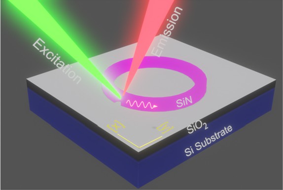
Schematic layout of coupled excitation and detection of cavity mode.Image credit: Authors of the study
Practically, this new method could mean that we may eventually be able to manufacture on-chip emitting devices for many photonic and quantum technologies without worrying about losses or instability. Like most electronic devices, this can lead to emitting devices also being integrated on a chip. The study has demonstrated the potential of silicon nitride to serve as a platform that can efficiently manipulate light on a very small scale.
Sharing insights on the research findings, Mr. Anuj Kumar Singh says that, “this work holds promise for several real-world applications in the near future like quantum computing, secure communications, and quantum sensing. While some applications may require additional research and development for practical implementation, others could be realized sooner.” Overall, the findings of this research present SiN as a key player in photonic technologies.
The manufacturing process using SiN comes with its drawbacks/errors, which can limit the performance of this novel technique. The researchers believe that improvements are possible in the material growth techniques and cavity design, leading to enhanced performance. “Our research contributes significantly, by enabling efficient light-matter interaction, controlled quantum emission, enhanced photonic devices, simplified integration, and the potential for quantum computing in quantum photonics. These advancements pave the way for groundbreaking applications in secure communication, ultra-fast computing, and other transformative technologies that will shape the future of science and technology,” adds Mr. Kishor Kumar Mandal.
In simpler words, a high-speed, secure, and energy-efficient digital future might be closer than we think!
Kishor Kumar Mandal, Laboratory of Optics of Quantum Materials, Department of Physics, Indian Institute of Technology Bombay, Mumbai, 400076, India
Anuj Kumar Singh, Laboratory of Optics of Quantum Materials, Department of Physics, Indian Institute of Technology Bombay, Mumbai, 400076, India
Brijesh Kumar, Laboratory of Optics of Quantum Materials, Department of Physics, Indian Institute of Technology Bombay, Mumbai, 400076, India
Amrita Majumder, Laboratory of Optics of Quantum Materials, Department of Physics, Indian Institute of Technology Bombay, Mumbai, 400076, India
Janhavi Jayawant Khunte, Laboratory of Optics of Quantum Materials, Department of Physics, Indian Institute of Technology Bombay, Mumbai, 400076, India
Anshuman Kumar, Laboratory of Optics of Quantum Materials, Department of Physics, Indian Institute of Technology Bombay, Mumbai, 400076, India