Transmission Electron Microscopy Facility (300 kV)@MEMS
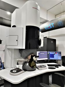
The transmission electron microscope is a 300kV high-resolution microscope with a field emission gun and excellent analytical performance. This facility is used for analysis of elemental composition by energy dispersive spectroscopy, diffraction for crystal structure determination and crystallographic studies.
Make and Model
Thermo Scientific, Themis 300 G3
Available mode for use
-
Conventional TEM mode
Scanning TEM mode
Spectrum Imaging (EDS)
Tomography
Local Orientation and Stress (A-Star) – to be installed with RIFC support.
Available detectors :
Super-X (EDS), Conventional TEM and STEM
Specifications/Features
-
Point resolution – 0.2 nm for TEM, 0.12 nm for STEM
Information limit – 0.18 nm
Minimum Brightness – 9.88 x 10⁷ A/m2srV
EDS energy resolution at Mn – 125 eV
Maximum spot drift – 0.45 nm/min
Application
-
Deformation in metals
Nano science/Nano Technology
Thin Films
Energy Science/Engineering
Chemical composition and quantification (TEM)
Elemental Mapping (STEM)
Tomography
Facility in-charge
Contact Email
temcoest[at] iitb[dot] ac[dot] inLocation
Room No. 027, Ground Floor, MEMS Department.
Other contact person(s)
- Prakash Ishte
Registration Link:
FEG featuring a high brightness and a high stability realizes structural imaging at atomic resolution.
Highly bright sub-nanometre sized probe enables us to perform an ultimately sensitive analysis of a sample at sub-nanometre resolution.
Super-X, an arrangement of 4 EDS detectors, for fast and reliable spectrum acquisition.
With optionally available piezo specimen drive system, specimen can be shifted at sub-nanometre resolution with a range of ± 1.2 μm.
A tomography holder for electron tomography application with tilt range of ±70o.
Local Orientation and Stress (A-Star) – to be installed with RIFC support.
Innovative scientific technologies used in today's nanotechnology are making remarkable progress. In research on localized strain measurement, novel materials such as carbon nanotubes, semiconductors and ceramics, as nanometre-scale evaluation and analysis are essential. This electron microscope is equipped with a field emission electron gun (xFEG) that produces high and is highly stable. This feature is essential for Nano-scale ultrahigh resolution analysis. HRTEM has an imaging mode that allows the imaging of the crystallographic structure of a sample at an atomic scale. Because of its high resolution, it is an invaluable tool to study Nano scale properties of crystalline material such as semiconductors, ceramics, metals, etc. HRTEM is the tool useful in imaging (semiconductor, core-shell nanoparticles, grain boundaries, etc.), to see structure details of nanotubes, nanowires, nanoparticles and so on.
1. R. Tripathi et al. ACS Appl. Nano Mater. 2022, 5, 12, 17767–17782
2. P. Gandharapu et al. Clean Technologies and Environmental Policy. 2023,
3. Vaibhav Verma et al. Carbon, Volume 209, 5 June 2023, 118007
4. B.S Kumar et al. Adv. Energy Mater. 2023, 2204407
5. Anagha Pradeep et al. Carbon Volume 201, 5 January 2023, Pages 1-11
6. I Biswas et al. Chem. Commun., 2023, 59, 4332-4335
7. B S Kumar et al. Chem. Mater. 2022, 34, 23, 10470–10483
8. Kankona Singha Roy et al., ACS Appl. Mater. Interfaces, 13(8) (2021) 9897-9907
9. Anagha Pradeep et al., Elec. Acta, 362 (2020) 137122.
10. P. Manikandan et al., MMTA, (2021) https://doi.org/10.1007/s11661-021-06337-y
11. Agrawal et al., MMTA, 52 (2021) 1465-1476.
12. Saurabh Kumar et al. Mater. Charac.,2023 199, 112822.
13. Aditya Prakash et al., IJP, 2023.
14. Saurabh Kumar et al., MMTA, 2023, 54A,1236-1251.
15. Soudip Basu, et al., Mater. Charac., 2023,197, 112704.
16. Sanjay Manda et al., MMTA, 2023, 54A, 562-576.
17. A. Sarkar et al., Mater. Charac., 2023,194, 112426, 1-15
- The bulk samples has to be of 3 mm diameter.
- The user has to collect TEM grids for powder samples from STEM lab.
- The user has to come for STEM analysis with prepared sample.
- The samples should be prepared on TEM grids of 3 mm size and sample thickness should be less than 100 nm for high resolution images.
- Any query related to your FEG-TEM analysis can be emailed to temcoest [at] iitb [dot] ac [dot] in ()
The samples should be dry and should withstand ultra-high vacuum
- Registration is online through drona interface.
- Intimation of appointment by email.
- New users are requested to contact first.
Cancellation/postponing a slot – at least 24 h earlier.