Unlocking High-Frequency Surface Acoustic Waves in Silicon: A New Frontier for Phononic and Quantum Devices
Surface acoustic waves (SAWs) −tiny elastic vibrations that travel along the surface of a solid−are the unsung heroes of modern wireless technology, powering the radio-frequency filters in every smartphone. As wireless communication advances towards 5G, 6G, and millimeter-wave (mm-wave) technologies, there is growing demand for compact, low-loss, and ultra-high-speed signal-processing devices compatible with existing silicon electronics. However, as the demand for faster communication and quantum-ready hardware grows, traditional methods for generating these waves are hitting a physical wall.
Researchers from the Indian Institute of Technology Bombay and the Raja Ramanna Centre for Advanced Technology have now demonstrated a breakthrough method to generate and control high-frequency SAWs directly in monolithic silicon. By utilizing higher-order acoustic modes and precise transducer engineering, the team has achieved frequencies up to 16.5 GHz with low signal loss, paving the way for a new generation of CMOS-compatible phononic devices.
The study appeared online May 25 in the journal Nano Letters.
The Scaling Challenge
Traditional SAW devices rely on piezoelectric materials, which convert electrical signals into mechanical vibrations. While effective, these materials are difficult to integrate with standard silicon-based electronics (CMOS). Furthermore, as frequencies push into the multi-GHz regime, the "fingers" of the interdigital transducers (IDTs) used to launch these waves must become impossibly small, leading to massive energy leakage and fabrication hurdles.
"The primary reason for SAW devices being built on piezo-actuation is that silicon is incompatible due to its lack of piezoelectricity," Arun Babu, the lead author of the study, explains. To bypass this, the team turned to optical actuation and extreme ultraviolet (EUV) diffraction.
A Clever Workaround: Higher-Order Mode Equivalency
One of the study's most significant findings is the equivalence of first- and second-order SAW modes. In simple terms, the researchers found that they could generate a second-order wave−which vibrates at twice the frequency of the fundamental wave−and that it behaves almost identically in terms of how it travels and fades away.
This discovery is a game-changer for manufacturing. It allows engineers to achieve 10 GHz or 15 GHz frequencies using larger, easier-to-fabricate transducers that would normally only produce 5 GHz or 7.5 GHz signals. The team established this equivalency across a wide range of frequencies (3.5–16.5 GHz) and lifetimes (14–0.6 ns).
Engineering Low-Loss Waves
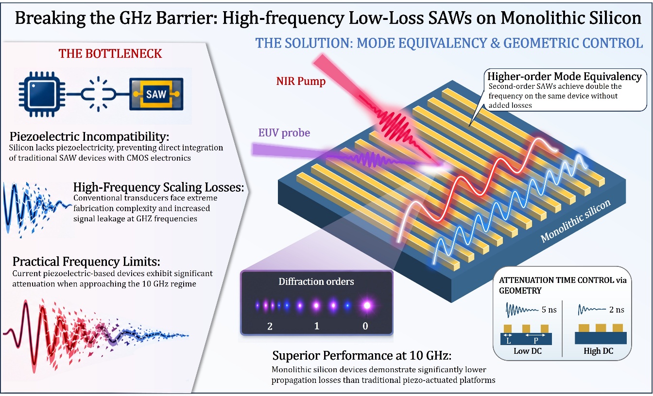
Figure 1: Researchers used an ultrafast laser pulse to create thermoelastic stress in nickel transducers on silicon, launching surface acoustic waves that are then "probed" by a beam of extreme ultraviolet light via diffraction. Image credit: Arun Babu
Surface acoustic waves inevitably lose energy as they travel, a phenomenon known as attenuation. The researchers discovered that they could "tune" how long these waves last by simply changing the transducer geometry, specifically the "duty cycle" or the width of the metallic lines compared to the space between them.
By optimizing this geometry, they achieved a 10 GHz SAW with a lifetime of approximately 5 nanoseconds. This represents significantly lower losses than those seen in traditional piezoelectric devices at similar frequencies. In fact, the propagation losses in their monolithic silicon platform were found to be remarkably low, making it an attractive alternative to current technology.
Why It Matters
This research provides a direct route to integrating high-speed "phononic" (sound-based) functionalities into mainstream semiconductor technology. Because the system is built on silicon and uses metallic transducers, it is theoretically compatible with the chips already found in computers and cars. Possible applications include: 5G/6G wireless technologies−enabling compact low-loss radio frequency filters, signals processors, and frequency control components for next-generation communication systems; Next-Generation Sensing−High-frequency waves are more sensitive to tiny mass changes, ideal for advanced biosensors; Phonon Lasers−The ability to sustain low-loss, high-frequency waves is a critical step toward practical solid-state acoustic lasers; Quantum Information−Low-loss SAWs can serve as "buses" to carry information between different parts of a quantum processor.
"Our work provides a timely route toward integrating phononic functionalities within mainstream semiconductor technology," said Dipanshu Bansal, Associate Professor in the Department of Mechanical Engineering at Indian Institute of Technology Bombay. By mastering the "geometry of sound," the team has opened a new door for high-frequency electronics that are both faster and easier to build.
This work was supported by the Anusandhan National Research Foundation (ANRF), erstwhile Science & Engineering Research Board (SERB) under Project No. CRG/2022/001317.
CITATION: A. Babu, M. Kumar, H. Singhal, A. Ansari, J.A. Chakera, and D. Bansal. “Control of High-Frequency Surface Acoustic Waves via Transducer Geometry and Higher-Order Mode Equivalency.” Nano Letters, 2026. https://doi.org/10.1021/acs.nanolett.6c01437