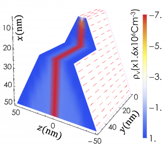
A novel route to achieve 2D carrier confinement in a wedge shaped wall structure made of a polar semiconductor has been demonstrated. Our theory reveals that the wedge shape leads to the development of charges of equal polarity on the two inclined facades of the wall. Polarisation induced negative (positive) charges on the facades can push the electrons (holes) inward for a n-type (p-type) material which results in the formation of a 2D electron (hole) gas at the central plane and ionised donors (acceptors) at the outer edges of the wall. The advantage of the 2D carrier gas formed this way over the conventional heterostructure based 2D systems is the significant suppression of ionised impurity scattering rate as a result of the natural separation of the carrier gas from the ionised impurities. A real life example is c-oriented wedge shaped GaN nanowall network grown by molecular beam epitaxy on sapphire substrates. In fact, electron mobility in this material is experimentally estimated to be several orders of magnitude larger than that is observed in GaN bulk.
A unique feature of this 2D channel is its ability to be formed in a plane perpendicular to the growth plane. One can thus envisage to fabricate large number of parallel 2D channels out of a single semiconducting film using a suitable lithographic and etching technique. This may offer an opportunity for large scale integration of 2D high mobility devices in future.
Prof. Subhabrata Dhar