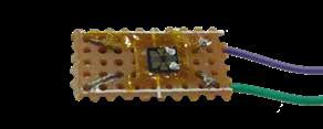
At the Photonics Laboratory in IIT Bombay, we are developing various photonic devices based on different spectroscopic techniques. They are tailored for various opto-electronic and sensing applications in the agricultural, healthcare and environmental sector. Multispectral ■ Modulate the band gap of graphene oxide (GO) and optimise it for desired sensing in characteristics optical range Novelty ■ Easy process exploiting electric field induced reduction approach for tuning the bandgap of GO leading to development of novel photonic devices Salient features ■ Photoresponsivity ranging from UV-Vis to near Infrared region having photocurrent of the order of μA ■ Surface of GO is easily functionalisable for various chemical and biochemical applications ■ Tunable photo-sensitivity in desired wavelength range extending from UV to near Infrared ■ The developed photonic micro-devices can easily be extended to prototype devices for various applications Applications ■ Broadband on-chip Photodetector (Fig. 1) ■ On-chip photonic sensing platform using spectroscopic techniques (Fig. 2)
Prof. T Kundu