A new method improves how metals connect with semiconductors by adding a very thin layer of black phosphorus in between. This layer helps electric current flow more easily or stop more effectively based on what the device needs. As a result, electronic parts like chips and sensors can work faster, use less power, and last longer.
The design also solves a common problem in semiconductor technology by better controlling how energy levels line up at the connection point. The black phosphorus layer has special properties that can be adjusted by changing its thickness. It’s made at room temperature, without using any harmful chemicals, making the process safer, cheaper, and easier to scale.
In many modern electronic devices, when metal connects with certain materials like Germanium (a type of semiconductor), the flow of electric current is blocked or slowed down due to a natural energy barrier. This issue, known as “Fermi-level pinning,” limits how efficiently these devices can perform, especially for high-speed or low-power electronics.
- Black Phosphorus Depinning Layer: This product uses a multilayer black phosphorus film that stops unwanted energy trapping, so electrons move freely.
- Tunable Contact Behavior: This feature lets designers switch between easy flow (Ohmic) or controlled barrier (Schottky) by changing substrate type.
- Low Resistance Interface: This product avoids bulky interlayers; its thin film keeps resistance low and power losses minimal.
- Simple Mechanical Exfoliation: This feature relies on peeling thin layers with tape— no complex chemical steps needed.
- Wide Compatibility: This product works with standard metals (like tungsten) and common semiconductors (like Ge), making it easy to adopt.
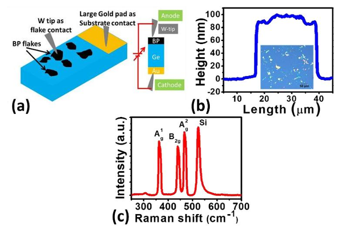
In the lab, researchers cleaned Germanium wafers, peeled on a ~100 nm black phosphorus film, then pressed a tungsten probe on top and a gold contact underneath. They measured electrical currents in a dark, enclosed station immediately after preparation. Microscopy, profilometry, and light-scattering tests confirmed film thickness and quality.
The technology has been tested in a laboratory setting. Researchers built a working version of the device and successfully showed that it improves electrical performance using this new method. All tests were done on real materials using standard lab equipment, and the results were measured and confirmed.
5
By slashing the wasteful resistance at tiny metal-semiconductor junctions, this innovation helps circuits switch faster while sipping far less power. In portable devices, that means noticeably longer run-times between charges—so smartphones, tablets, and wearables can last through a full day (or more) of heavy use. In large-scale computing centers, lower power draw reduces electricity bills and eases cooling demands, cutting both operational costs and carbon footprints. Cooler-running chips are also more reliable, shrinking the risk of heat-related failures. Altogether, the technology paves the way for slimmer, lighter electronics, extended-life batteries, and greener data processing—delivering clear benefits for end users, manufacturers, and the planet.
- Semiconductor and chip manufacturing
- Electronics and computing hardware
- Sensor and communication device industries
- Advanced material engineering research
Geography of IP
Type of IP
201921036221
538912

