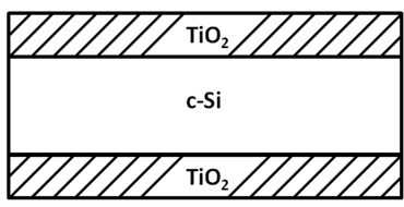
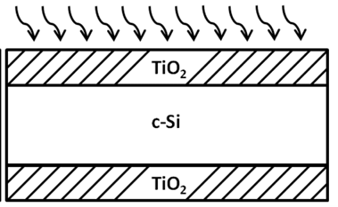
A new way to boost solar cell performance uses a very thin layer of titanium dioxide (TiO₂) coated on silicon and treated with hydrogen plasma at room temperature. This gentle process seals tiny defects on the silicon surface without damaging the material, so more electricity can flow out when sunlight hits the cell. Tests in the lab show the treated devices deliver higher voltages, lower energy loss, and better overall efficiency compared to traditional heat-baked coatings.
Traditional solar cell manufacturing processes often require high-temperature treatments, which can be expensive, energy-intensive, and may damage delicate materials. These heat-based methods also create tiny imperfections that reduce the efficiency of the solar cells. Finding a simpler and low-energy way to make solar cells more efficient is a major challenge.
- Low-Temperature Energy-Saving Process: This product uses hydrogen plasma at room temperature instead of high-heat treatments, significantly reducing the energy required during manufacturing and lowering overall production costs.
- Defect Elimination for Better Efficiency: This feature allows hydrogen atoms to bond with exposed spots on the silicon surface, effectively sealing defects that would otherwise cause energy loss and reduce solar cell performance.
- Maintains Amorphous Film Structure: This product preserves the ultra-thin titanium dioxide film in a smooth, glass-like (amorphous) state, avoiding cracks or grain boundaries that could slow down or trap electrons.
- Improved Electrical Performance: Devices made using this method show measurable gains in voltage, reduced current leakage, and better charge collection compared to conventional heat-treated devices.
- Eco-Friendly and Scalable Manufacturing: By avoiding high temperatures and complex steps, this process supports cleaner, greener manufacturing and can be easily scaled up, especially in areas with limited industrial infrastructure.
In the lab, silicon wafers were coated on both sides with a 2–8 nanometer TiO₂ film using atomic layer deposition. The wafers then sat in a vacuum chamber, where hydrogen gas was energized into plasma and applied for five minutes at 1 Torr pressure. After treatment, the sample behaved like a working solar diode: it let light through, generated current, and showed clear improvements in voltage and leakage tests.
This technology has been successfully demonstrated in a laboratory using real solar cell components. The results showed significant improvements over traditional heating methods. It is currently at an early prototype stage, with solid proof of concept and lab validation.
4
By significantly reducing the amount of energy needed during the manufacturing process, and at the same time boosting how well solar cells work, this technology has the potential to make clean electricity much more affordable. Since it avoids high-temperature treatments, it cuts down on factory energy costs and greenhouse gas emissions typically associated with traditional production methods. This cleaner and simpler process makes it easier to produce efficient solar panels even in places that lack advanced infrastructure or heavy-duty industrial equipment. In particular, developing regions or rural areas where power resources and industrial capacity may be limited can benefit greatly from this low-heat, low-cost approach. Ultimately, this innovation supports the global shift toward sustainable energy by making solar power more accessible and environmentally friendly for everyone.
- Next-generation solar module manufacturing
- Photovoltaic research and development
- Semiconductor device fabrication
- Clean-energy equipment suppliers
Geography of IP
Type of IP
201721041280
519431


