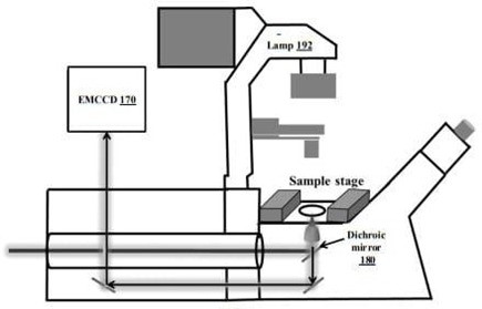
This invention describes a method for patterning 3D nano-microstructures of sub-wavelength resolution with two photon lithography using an apparatus. The method includes spin coating, by the apparatus, a photo-patternable resin over a transparent substrate and receiving, by the apparatus, dimensions of the photo-patternable resin for patterning the 3D nano-microstructures. Further, the method includes determining, by the apparatus, whether the dimensions of the photo-patternable resin is greater than a dimensional threshold and patterning, by the apparatus, in a first translation stage using the two-photon lithography when the dimensions of the photo-patternable resin is greater than the dimensional threshold and a second translation stage when the dimensions of the photo-patternable resin is not greater than the dimensional threshold. Further, the method also includes removing, un-polymerized photo-patternable resin from the transparent substrate to obtain the 3D nano-microstructures of the sub-wavelength resolution in a single exposure step.
Two-photon lithography (TPL) holds significant potential for high-resolution 3D micro- and nanofabrication, but current systems are limited by their inability to consistently achieve sub-wavelength resolution, lack of flexibility in switching between nano- and micro-scale structures, and restricted compatibility with diverse photoresists due to fixed operational wavelengths. Additionally, the absence of real-time monitoring, feedback control, and distortion compensation leads to inaccuracies and structural deviations during fabrication. These limitations hinder the precision, repeatability, and broader applicability of TPL in advanced fields such as biomedicine, microfluidics, and photonics.
- Compact and Cost-Effective Design: The system is engineered to be significantly smaller and more affordable than conventional femtosecond laser fabrication setups, making it accessible for wider adoption.
- Sub-Wavelength Precision Fabrication: It enables the creation of intricate 3D micro- and nano-structures with extremely high spatial resolution, crucial for advanced biomedical and photonic applications.
- Fully Integrated and Modular System: It incorporates all essential components - including a femtosecond laser, beam modulators, optical switches, translation stages, and controllers - within a cohesive and user-friendly setup.
- Alignment-Free Operation: It is designed to eliminate the need for frequent optical realignment, thereby improving operational stability and reducing technical barriers for non-expert users.
- Real-Time Monitoring Capability: It is equipped with an in-built monitoring system that allows users to visualize the fabrication process live, enhancing precision, quality control, and reproducibility.
- Versatile and Application-Oriented: It supports rapid prototyping across multiple domains such as biomedical engineering, micro-optics, tissue engineering, and environmental sensing, making it suitable for diverse industry needs.
- Ideal for Research and Startups: Its affordability, portability, and ease of use make it an excellent tool for academic institutions, small laboratories, and emerging startups, especially in resource-constrained settings.
The prototype integrates a femtosecond laser source with advanced beam modulators, optical switches, dual translation stages, a high-precision microscope objective, a real-time monitoring unit, and an integrated controller. This comprehensive setup enables precise and controlled laser-based microfabrication. The functional prototype has successfully demonstrated the fabrication of complex three-dimensional structures with sub-wavelength accuracy, validating its effectiveness for high-resolution applications in various scientific and industrial domains.
The technology is at the stage of early prototype development and/or validation in relevant environment.
5
The technology enables low-cost, high-resolution fabrication of biomedical scaffolds, microneedles, and drug delivery systems, significantly advancing healthcare solutions. It supports rapid prototyping of optical components for miniaturized photonic devices, fostering innovation in communication and sensing technologies. By enhancing access to precision manufacturing tools for academia and startups, especially in emerging economies, it promotes inclusive technological development and innovation. Furthermore, it facilitates progress in critical areas such as tissue engineering, microsensors, and environmental microdevices, contributing to improved quality of life and sustainable development.
- Biomedical Engineering: Tissue scaffolds, organ-on-chip systems, microneedles
- Photonics and Optoelectronics: Photonic crystals, waveguides, micro-optics
- Aerospace and Defense: Lightweight microstructures, sensors, and actuator systems
- Microfluidics: Lab-on-a-chip, microreactors
- Material Science: Functional metamaterials, responsive polymers
- Education and Research: Precision nanofabrication for academic labs and prototyping
Geography of IP
Type of IP
202221011509
432231

