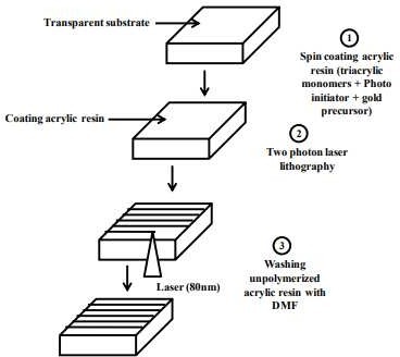
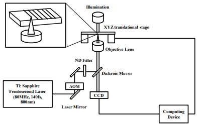
This invention describes a method for fabricating a metal polymer composite of sub-wavelength dimensions. The method includes preparing an acrylic resin, where the acrylic resin contains a mixture of two triacryclic monomers, a photo initiator and a gold precursor. Further, the method includes coating a transparent substrate with the acrylic resin and irradiating the transparent substrate by performing a two-photon lithography using a laser source. Further, the method also includes removing unpolymerized acrylic resin and unexposed metal precursor to reveal a pattern formed by the two-photon lithography.
Figure (1) Illustrates a method for fabricating metal-polymer composite of sub-wavelength dimensions using dyeless two photon lithography technique; (2) Illustrates a method for performing two photon lithography using a laser source for fabricating 2D and 3D metal-polymer composite pattern on the transparent substrate
Precise micro- and nano-scale structuring of polymer materials is critical for applications in photonics, sensors, and bio-devices. However, achieving consistent feature sizes with high resolution and minimal variation remains a challenge, particularly when integrating functional materials like gold nanoparticles into polymer matrices. Conventional photopolymerization methods often suffer from high variability in line widths and increased ablation risk at higher energies.
- Gold-Doped Photopolymer Matrix: The technology utilizes controlled gold nanoparticle loading (0 to 10 wt%) within the polymer matrix, enabling tunable optical and physical properties during fabrication.
- Precision Laser Direct Writing: It employs laser-based direct writing with constant periodicity (1.5 μm), achieving highly accurate and reproducible micro- and nano-scale structures.
- Reduced Line Width with Increased Gold Loading: It demonstrates that higher gold concentrations result in narrower line widths, enhancing feature resolution and miniaturization capabilities.
- Optimized Energy Threshold: It identifies an optimal laser power threshold (~186 mW) for clean, non-ablative writing, ensuring process stability and reducing material damage.
- Improved Photoreduction Efficiency: Gold ions participate actively in the photoreduction process, leading to sharper pattern definition by balancing the photo initiator’s role between polymerization and metal reduction.
- Versatile and Scalable Fabrication Platform: It is adaptable to various gold concentrations and laser parameters, making the technology suitable for diverse applications in photonics, sensing, and bioengineering.
The prototype consists of a photopolymer matrix doped with varying gold loadings of 0 wt%, 1 wt%, 5 wt%, and 10 wt%. Fabrication is achieved through laser-based direct writing, maintaining a constant grating periodicity of 1.5 μm while controlling the laser power. Scanning Electron Microscopy (SEM) characterization of the fabricated gratings confirms that higher gold concentrations result in reduced line widths. The process is optimized with a clean writing threshold power of approximately 186 mW for the gold-doped polymers, ensuring precise patterning without sample damage.
The technology is at early prototype development and/or validation in relevant environment.
4
The developed technology has broad societal impact across domains. It enables fabrication of miniaturized, high-precision optical components for advanced photonic devices, vital to next-gen communication and sensing. In medical diagnostics, it aids lab-on-chip development with precise microfluidic and biosensor structures, enhancing point-of-care testing. The method also supports sustainable manufacturing by minimizing energy use and material waste through controlled fabrication. Additionally, it fosters innovation in education and research, empowering institutions and industries in nanofabrication and material science.
- Photonics and Optoelectronics
- Biomedical Devices & Lab-on-a-Chip Systems
- Microfluidics
- Flexible Electronics
- Sensor Technology 3D Micro- and Nano-Fabrication
- Material Science & Polymer Engineering
Geography of IP
Type of IP
202021017407
405852


