This invention provides a de-serializer architecture using a synchronization controller and an N-phase clock generator for converting a stream of serial data into a plurality of streams of parallel data. The de-serializer eliminates the need for CDR/DLLs circuits, resulting in a simpler hardware design and higher data rate. The N-phase clock generator ensures accurate synchronisation of data bits, and the synchronisation controller generates synchronisation pulses to align the clock phases with the data bits.
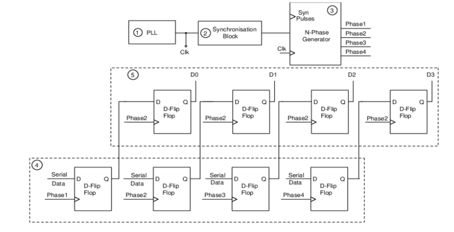
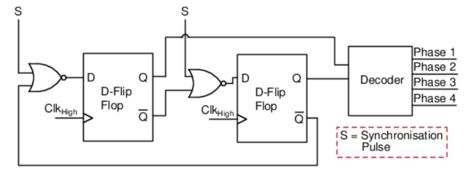
Figure (1) Architecture of Serializer/De-serializer (SERDES) to show the conventional setup; (2) Schematic diagram illustrating the architecture of the de-serializer comprising synchronization controller and 4-phase clock generator; (3) Schematic diagram of the 4-phase clock generator for clarity in its operational mechanism
The conventional de-serializer systems require complex architectures with phase-locked loops (PLLs) and clock data recovery (CDR) or delay locked loops (DLLs) to synchronize serial data, which limits the operating frequency range and increases complexity. The proposed invention aims to address these limitations by providing a de-serializer that eliminates the need for CDR/DLLs circuits, thereby simplifying the hardware and increasing the data rate for the same clock frequency.
- Synchronisation Controller: A synchronisation controller generates synchronisation pulses periodically using information from the clock sent by the serializer, ensuring accurate alignment of clock phases with data bits.
- N-Phase Clock Generator: An N-phase clock generator produces multiple phases of clock using the information from the clock and synchronisation pulses, enabling parallel data generation.
- Wideband Operation: The use of N-phase clock generators allows for wideband operation, increasing the operating frequency range.
- Reduced Overheads: The proposed design simplifies the hardware, reduces chip area and power consumption for a given data rate and clock frequency.
The prototype consists of a serialiser and deserialiser module. The serializer transmits serial data along with clock information, which is received by the de-serializer. The de-serializer includes a clock receiver to extract the clock information, a synchronisation controller to generate synchronisation pulses, and an N-phase clock generator to produce multiple clock phases. The first set of N flip-flops aligns each clock phase with the corresponding data bit, and the second set of N flip-flops generates parallel data streams using the common phase of the clock.
A semiconductor chip-based prototype has been demonstrated.
4
This technology enables more efficient data processing in various applications, reducing the complexity and cost of electronic systems. It supports the development of high-performance computing platforms, improves energy efficiency, and enhances the performance of high-speed interface ICs. Additionally, it contributes to the advancement of indigenous microelectronics research and development capabilities.
- Data Converters
- Field Programmable Gate Arrays (FPGAs)
- Network Processors
- Graphics Processors
- Embedded Systems
- High-Speed Communication Systems
Geography of IP
Type of IP
202121008597
552776


