This invention discloses an N-channel power Nano-Electro-mechanical FET (NEMFET) that improves on-current and speed compared to conventional D-MOSFETs by eliminating interface traps at the channel/dielectric interface. The NEMFET uses a suspended gate design with air or hybrid dielectric stacks, enhancing electron mobility and reducing on-resistance. The device can be fabricated using SiC or Ga2O3 as the semiconductor material, and the hybrid dielectric stack further increases the electric field and carrier concentration in the channel.
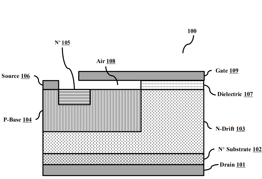
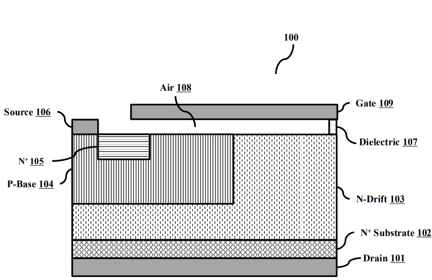
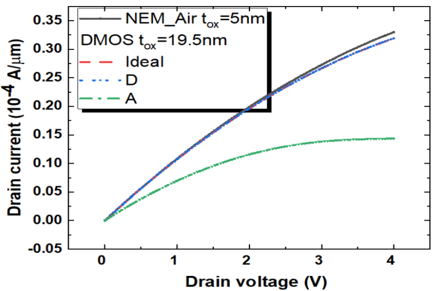
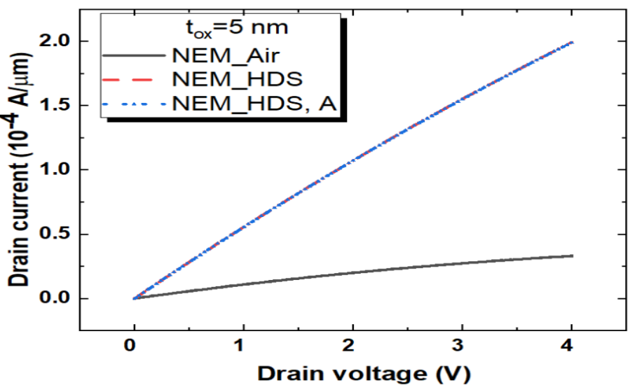
Figures (1a) & (1b) Depict the vertical power NEMFET with three contacts, showing the difference between NEM_HDS and NEM_Air; (2) Depicts the output characteristic of DMOS and NEM_Air, highlighting the improvement in on-current; (3) Depicts the output characteristic of NEMFET with two types of dielectric stack (Air and HDS), showing the significant improvement with the hybrid dielectric stack
The core problem addressed by this invention is the limitation in the on-conductance and speed of conventional MOSFETs due to interface traps at the semiconductor/dielectric interface. These traps reduce electron mobility, increase on-resistance, and lower on-current specifications. The invention aims to improve the on-current and speed of power devices by using a suspended gate design in N-channel Nano-Electro-mechanical FETs (NEMFETs), which eliminates interface traps and enhances channel mobility.
- Suspended Gate Design: The invention eliminates interface traps at the channel/dielectric interface, improving electron mobility and on-current.
- Hybrid Dielectric Stack: It increases the electric field and carrier concentration in the channel, further enhancing device performance.
- Air as Gate Dielectric: It passivates the semiconductor surface, neutralizing interface traps and improving channel mobility.
- Enhanced On-Current: It achieves a 40% improvement in on-current through the application of a novel hybrid dielectric stack.
- Compatibility with SiC and Ga2O3: It can be fabricated using either SiC or Ga2O3 as the semiconductor material, offering flexibility in material choice.
The prototype consists of a vertical power NEMFET with three contacts: drain, source, and gate. The device is fabricated on a highly doped N+-type substrate (SiC or Ga2O3) with an n-type epitaxial layer forming the N-drift region. A p-Base region and an N+ source region are formed through high-temperature ion implantation. The gate dielectric can be either air (NEM_Air) or a hybrid dielectric stack (NEM_HDS), with the gate contact patterned using deposition, photolithography, and subtractive etch processing. The source and drain contacts are formed by metallization. The hybrid dielectric stack significantly enhances the electric field and electron density in the channel, leading to improved device performance.
Proof of Concept
3
This technology enables higher speed and miniaturization of power devices, reducing the size of passive components and entire circuitry. It enhances the performance of power electronics, making them more efficient and reliable for high-power density and temperature applications. This innovation advances the development of next-generation power devices, benefiting industries such as automotive, renewable energy, and consumer electronics.
- Power Electronics: High-speed, high-efficiency power devices
- Automotive Industry: Compact and efficient power management systems
- Renewable Energy: Enhanced performance in power conversion systems
- Consumer Electronics: Smaller, more efficient electronic devices
- Industrial Automation: Reliable and efficient power control systems
- Telecommunications: High-performance power amplifiers and converters
Geography of IP
Type of IP
202021055965
533520
