Embodiments herein disclose a planar junctionless N-channel power transistor (JLT) designed to improve carrier transport using a bulk channel. The JLT structure is made of Silicon Carbide (SiC) or Gallium Oxide (Ga2O3) and is suitable for low to medium voltage applications. The device circumvents the interface trap problem of SiC-based power MOSFETs, leading to enhanced on-current and reduced on-resistance.
The invention addresses the challenges associated with scaling traditional Metal Oxide Semiconductor (MOS) Field Effect Transistors (MOSFETs) and the limitations of Silicon Carbide (SiC) power MOSFETs, particularly the low channel mobility due to interface traps. It proposes a planar junctionless transistor (JLT) structure using SiC or Gallium Oxide (Ga2O3) to improve carrier transport and enhance device performance in low to medium voltage applications.
- Planar JLT Structure: The innovation utilizes a planar design to simplify fabrication and improve carrier transport.
- Bulk Channel Transport: It enhances carrier mobility by using the bulk of the semiconductor material.
- SiC or Ga2O3 Material: It leverages wide bandgap semiconductors for high power-density and temperature operation.
- Improved On-Current: It reduces on-resistance and increases on-current by avoiding interface traps.
- Low to Medium Voltage Applications: It is suitable for driver circuits, LEDs, and DC microgrids.
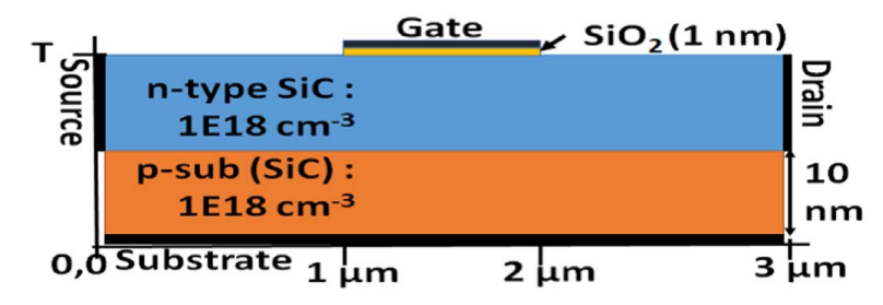
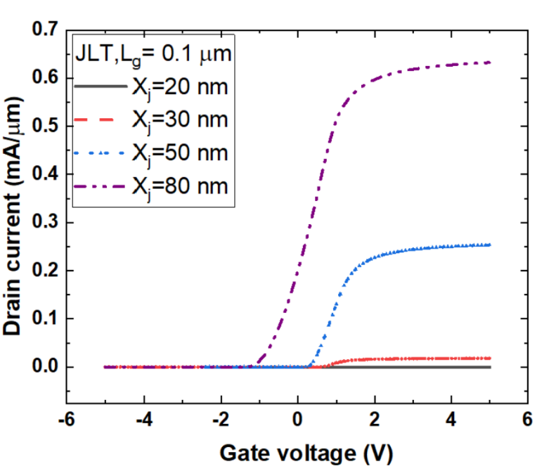
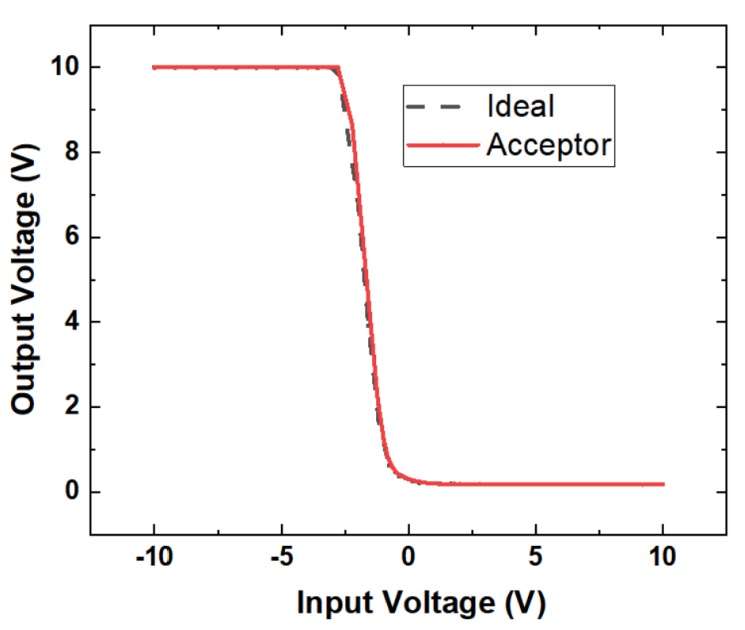
The prototype consists of a p-type SiC substrate with an epitaxially grown n-type SiC layer. A Silicon dioxide (SiO2) layer is deposited on a portion of the n-type layer, and contacts (gate, source, drain, and substrate) are formed by metallization. The device is tested in a common source configuration, demonstrating improved transfer and switching characteristics. The n-type layer thickness and substrate voltage are varied to optimize performance, and the device shows a maximum intrinsic speed of 5 GHz.
Proof of Concept
3
This technology enhances the performance of power devices in low to medium voltage applications, reducing energy consumption and improving efficiency in driver circuits for LEDs, DC microgrids, and auxiliary devices of EVs. It advances the development of green energy technologies and compact power-switching circuitry.
- Driver Circuits for LEDs: Enhances efficiency and reliability
- Single-Photon Avalanche Diodes (SPAD): Improves detection speed and accuracy
- X-ray Detectors: Enhances sensitivity and response time
- DC Microgrids: Reduces power loss and improves stability
- Auxiliary Devices of EVs: Enhances performance and efficiency
- Sensors: Improves signal-to-noise ratio and response time.
Geography of IP
Type of IP
202021048232
516365


