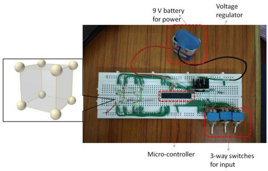
This invention presents an interactive optical system designed to represent motifs in a 3D plane. It features three-way switches corresponding to 3D Cartesian coordinates, multiple light sources connected to these switches, and a microcontroller that detects switch configurations representing Miller indices. Based on this input, the microcontroller controls the lighting of specific LEDs to visually represent motifs in the lattice planes.
In solid-state chemistry and materials science, understanding the 3D arrangement of atoms in crystal structures is vital for grasping concepts like Bravais lattices and structure-property relationships. Conventional molecular model kits are static and lack the ability to dynamically represent atomic positions or crystallographic planes such as Miller indices, making visualization difficult for learners. There is a clear need for an interactive, dynamic visualization system that allows real-time representation of atomic motifs and planes, enabling intuitive understanding of spatial relationships through user-controlled inputs and immediate feedback.
- Interactive Representation of Miller Planes: The innovation uses a combination of analog voltage inputs via three-way switches to intuitively select Miller indices, allowing for real-time visualization of lattice planes in 3D.
- Microcontroller Based Automation: Pre-programmed Atmega328P microcontroller detects input and lights up corresponding LEDs, representing motifs in a crystal structure.
- Voltage Mapping Technique: It makes innovative use of analog voltage levels (5V, 2.5V) to encode binary-like inputs without the need for complex user interfaces.
- Modular Design: It has easily reconfigurable LED and switch mappings via minor code changes - adaptable for various lattice structures or chemical models.
- Low-Cost and Educational: It is built using basic electronic components, making it affordable and accessible for educational institutions.
- Expandable Chemistry Visualization: The system can be adapted to simulate chemical reactions, resonance structures, and molecular dynamics (e.g., benzene resonance, Friedel-Crafts reactions).
The prototype uses an Atmega328P microcontroller pre-programmed to detect Miller index inputs through three 6-pin, three-way switches, each representing the x, y, and z Cartesian coordinates with voltage levels of 5V and 2.5V to encode the indices. Powered by a 9V battery and stabilized with an IC 7805 voltage regulator providing a constant 5V supply, the circuit includes a 16 MHz crystal oscillator with capacitors for timing, and resistors used in voltage dividers and to ground analog pins, preventing floating inputs. LEDs represent the eight corner atoms of a simple cubic lattice, lighting up based on the microcontroller’s stored Miller index data. The entire setup is built on a breadboard with connecting wires, allowing easy reconfiguration and visualization of 3D lattice planes through the lighting of motifs.
The product based on this technology has been developed and is being used by KV, IITB, as a teaching aid for solid-state chemistry.
5-6
This innovative interactive optical system significantly improves the visualization of complex crystallographic and chemical structures, making abstract 3D concepts more accessible and easier to understand. By enhancing STEM education with real-time, intuitive representations, it supports learners who face challenges in spatial reasoning. Its affordable and modular design encourages adoption across educational institutions, promoting scientific literacy, skill development, and fostering indigenous innovation aligned with societal goals of advancing education and STEM awareness.
- Education Technology (EdTech)
- Chemistry and physics labs
- Engineering education (Materials Science, Nanotechnology)
- Scientific Visualization
- Crystallography and solid-state physics research
Geography of IP
Type of IP
202121059330
424981

