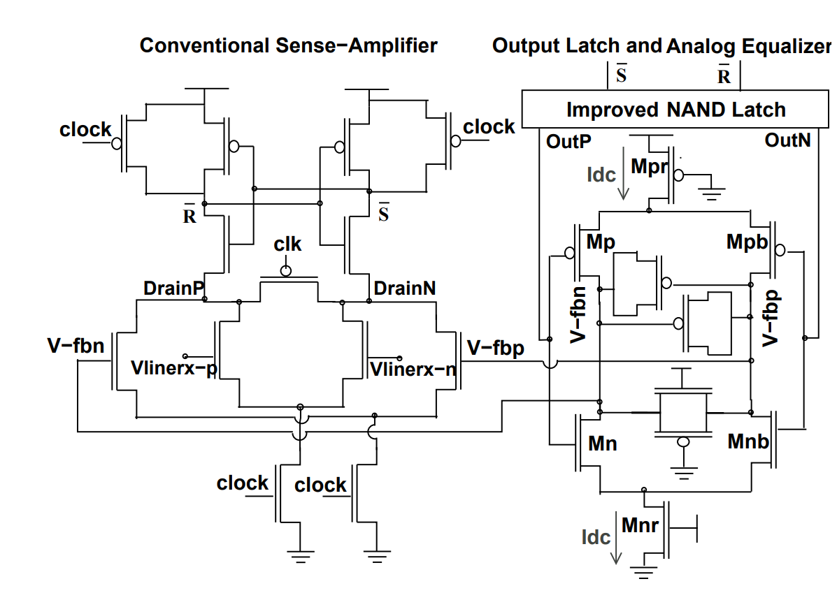
The invention proposes a signaling scheme for high-speed, low-power, and robust communication over long on-chip wires. It integrates a capacitively coupled transmitter with weak drivers and a novel analog equalizer-based receiver using a conventional sense amplifier flip-flop. The scheme operates at 3.45 Gbps over 10 mm wires while consuming only 0.107 pJ/bit. Designed in 90 nm CMOS, it remains effective across process and temperature variations, offering a significant advancement in energy-efficient on-chip communication.
Conventional long-wire communication on chips requires buffer insertion, leading to excessive power consumption. Emerging needs in modern high-speed chips demand alternatives that ensure high data rates, low power consumption, and robustness to process variations.
- Capacitively Coupled Transmitter: The proposed signaling scheme introduces a differential transmitter using tapered inverter chains and coupling capacitors, which enable efficient signal driving over long wires without repeaters.
- Weak Driver Integration: Weak drivers controlled by bias generators ensure minimal current draw, significantly lowering power consumption.
- Robust Analog Equalizer: The receiver employs an innovative analog equalizer with a low-pass filter that mimics channel behavior, improving throughput and robustness to previous-bit interference.
- Improved Flip-Flop Design: A conventional sense amplifier-based flip-flop enhances speed and reduces power compared to double-tail counterparts, supporting high data rates.
- Process Variation Tolerance: Design techniques such as transmission gate termination and differential signaling maintain consistent performance across process corners and intra-die variations.
The prototype is implemented using 90 nm CMOS technology. It includes a capacitively coupled transmitter with tapered inverter chains, series MOS capacitors, and weak current drivers. The receiver comprises a sense amplifier-based flip-flop and an analog equalizer with a low-pass filter for enhanced signal reconstruction. The system achieves 3.45 Gbps data rates over 10 mm wires, consuming 0.107 pJ/bit, and demonstrates stability under process variations, intra-die mismatches, and elevated temperatures (up to 90°C). Monte Carlo simulations confirm robust bit-error performance at data rates up to 3 Gbps.
A high-speed, low-power signaling scheme for long on-chip wires has reached the complete specification stage, achieving 3.45 Gbps data rates with only 0.107 pJ/bit energy consumption, and has demonstrated robustness under process and temperature variations.
3
The invention addresses energy-efficient high-speed on-chip communication, essential for modern electronics, from smartphones to servers. It contributes to reduced power consumption and enhanced performance in integrated circuits.
- High-speed digital communication
- System-on-chip (SoC) designs
- ASIC design and manufacturing
- Low-power VLSI systems
- Data center and high-performance computing chips
Geography of IP
Type of IP
2000/MUM/2012
369686

