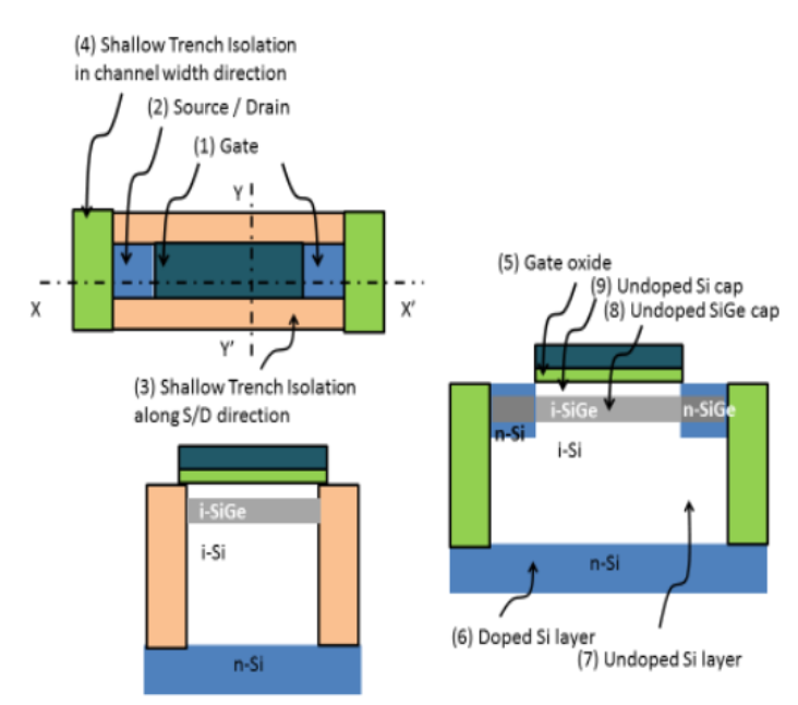
A capacitor-less dynamic random access memory (DRAM) comprises a n-type semiconductor, a plurality of intrinsic semiconductor layers stacked above said n-type semiconductor, said intrinsic semiconductor layers are walled between a pair of Shallow Trench Isolation (STI) layers over said n-type semiconductor, a gate region separated by a gate oxide layer from said intrinsic semiconductor layers and a source region and a drain region formed by wrapping two extreme side walls of said second intrinsic semiconductor layer with doped semiconductors.
Existing DRAM cell technologies, including vertical and planar capacitor-less designs, suffer from limitations such as high variability in threshold voltage and the requirement for expensive SOI wafers. There is a need for a planar bulk capacitor-less DRAM with low threshold voltage variability and immunity to random dopant fluctuations.
- Planar bulk capacitor-less DRAM design - cost-effective planar bulk design
- Si/SiGe/Si hetero-structure for hole confinement
- Impact ionization-based hole-generation
- Reduced threshold voltage variability
- RDF immunity through dopant profile engineering - Immunity to random dopant fluctuations
- High-k dielectric gate materials
- Improved performance and reliability
- Enhanced charge storage and retention
The prototype consists of a MOSFET structure with an n+ well, intrinsic Si/SiGe/Si layers, Shallow Trench Isolation (STI) layers, and a gate region with high-k dielectrics. The design demonstrates charge storage and retention in a planar bulk configuration, showing improved threshold voltage stability and performance.
The experimental memory functionality has been successfully demonstrated. This invention is in its stage of programming scheme optimization and endurance characterization for DRAM application.
3
The invention can lead to more reliable and cost-effective memory devices, enhancing the performance of consumer electronics, computing devices, and embedded systems. It supports advancements in semiconductor technology, contributing to the development of high-performance, low-power memory solutions.
- Dynamic Random Access Memory (DRAM) in computers and electronic devices
- High-density memory applications
- Embedded DRAM in system-on-chip (SoC) designs
- Non-volatile memory applications with charge trap flash integration
Geography of IP
Type of IP
1976/MUM/2015
507960

