This innovation is an inductor-less Low-Noise Amplifier (LNA) designed for low power, wideband applications, incorporating dual-stage noise cancellation and linearity modes. The LNA features complementary common gate (CG) and common source (CS) transistors, a feedback manager, and a buffer manager to improve noise performance and signal integrity without using external inductors.
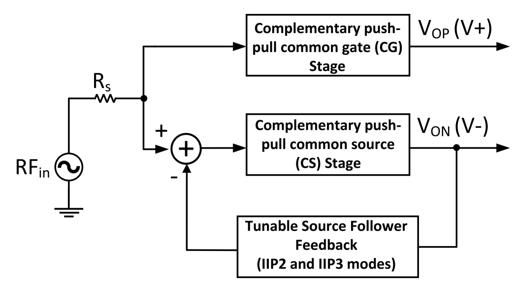
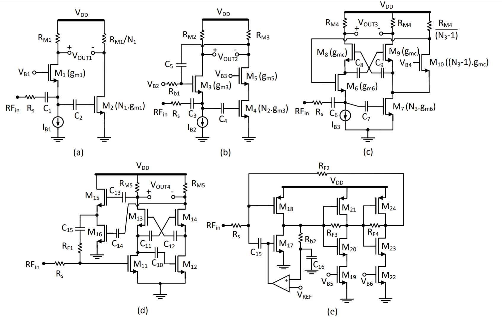
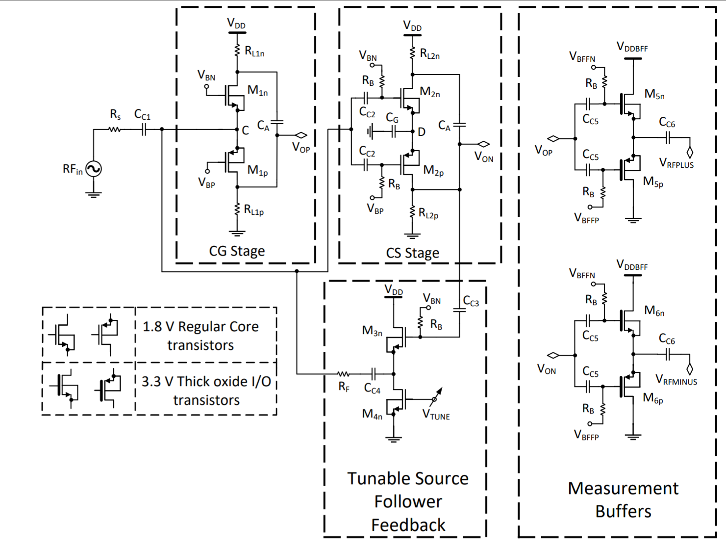
Figures (1) Conceptual diagram of proposed complementary CS-CG LNA; (2a) Traditional CS-CG LNA (2b) Traditional gm-boosted CS-CG LNA (2c) gm-boosted CS-CG LNA with auxiliary CS path (2d) Balun LNA with source follower feedback (2e) Complementary balun LNA with global shunt feedback; (3) Complete schematic of the proposed balun LNA with measurement buffers
Traditional wideband LNAs suffer from high noise figures and poor linearity, which are exacerbated by the use of baluns or inductors. These components consume significant power and degrade performance, especially in sub-GHz IoT applications requiring low power consumption and high efficiency.
- Inductorless compact design: This innovative design eliminates the need for inductors, reducing on-chip area and losses, as well as simplifies integration into RF receiver chains.
- Dual-stage noise cancellation: It utilizes both CG and CS stages to enhance noise performance.
- Complementary transistors: Both pMOS and nMOS transistors are used in CG and CS stages for balanced performance.
- Feedback manager: It incorporates feedback transistors to generate a feedback signal, enhancing noise cancellation and linearity without the use of inductors, ensuring better signal quality.
- Buffer manager: It combines in-phase and out-of-phase signals to generate differential output signals, improving signal integrity.
- Low power consumption: The design is optimized for low power use, suitable for IoT applications.
The LNA comprises a CG stage with complementary transistors, a CS stage with complementary transistors, a feedback manager for noise cancellation, and a buffer manager for signal output. The prototype would include capacitors for partial noise cancellation and the configuration to ensure complete noise cancellation through differential output.
The simulations of the proposed system have been completed successfully.
3
The technology provides efficient, low-power solutions for IoT and wireless communication, enabling longer battery life and more reliable performance in devices. This contributes to the advancement of smart technologies and connected devices, improving everyday life and promoting sustainable technology usage.
- RF receivers: Suitable for low-power RF receiver applications
- Telecommunications: Can be used in various telecommunication devices requiring efficient signal amplification
- Internet of Things (IoT): Useful particularly in sub-GHz wireless bands
Geography of IP
Type of IP
202221001348
456805


