This novel circuit aims to provide precise measurements of time delays in digital circuits, particularly in memory chips, by using programmable delay elements. The invention comprises of the following two main components.
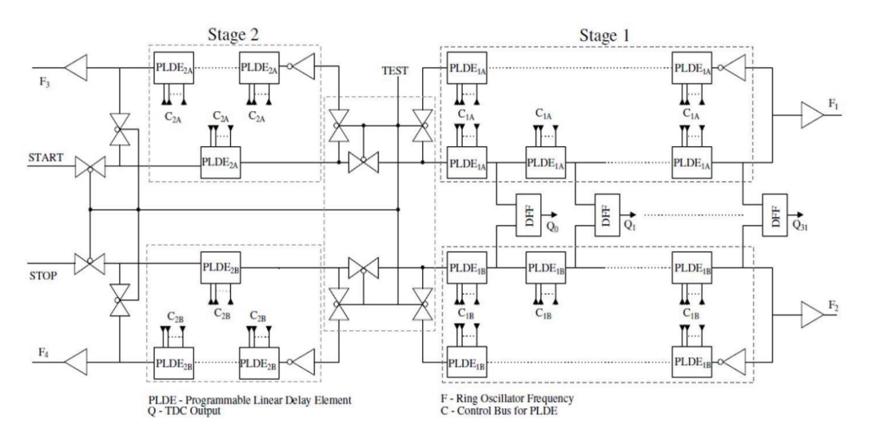
- Time to Digital Converter (TDC): The TDC converts time intervals into digital data. It uses two stages of delay elements to measure time intervals. The first stage consists of primary delay elements with a larger step size, while the second stage includes secondary delay elements with a smaller step size. Both stages have multiple ring oscillators (loops of delay elements), which can operate in three modes: test, calibration, and functional. In the test mode, the ring oscillators are separated to check functionality.
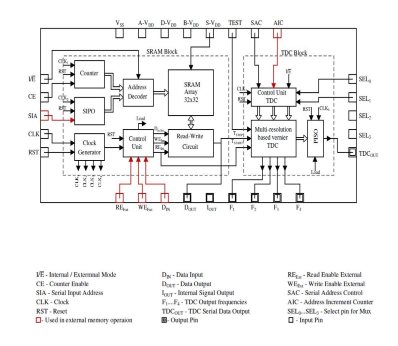
- Integrated circuit for measuring Static Random Access Memory (SRAM) delay: The integrated circuit for measuring SRAM delay is designed to measure delays within SRAM on a chip. It combines the TDC with an SRAM block. The TDC block has primary and secondary delay elements arranged in ring oscillators, a control unit for managing the TDC, and a parallel-to-series converter for processing the output data. The SRAM block includes an array of memory cells and can operate in modes for both internal chip memory and external memory interaction.
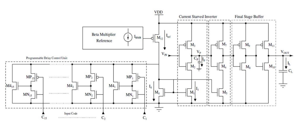
Figure (1) A schematic block diagram of an integrated circuit for measuring on chip delay of a static random access memory (SRAM) in an exemplary embodiment of the present disclosure; (2) A schematic of the time to digital converter in accordance with the exemplary embodiment of the present disclosure; (3) A programmable linear delay element used for the time to digital converter in accordance with the present disclosure
Design a highly precise time to digital converter (TDC) that can be effectively integrated into an integrated circuit (IC) for measuring on-chip delays in static random-access memory (SRAM).
- Multi-Resolution TDC: The invention features a multi-resolution based TDC for precise on-chip delay measurement in SRAM.
- Programmable Delay Elements: It includes primary and secondary programmable linear delay elements arranged in multiple ring oscillator units for flexible step sizes.
- Operating Modes: The TDC operates in test, calibration, and functional modes, with separated ring oscillator units during the test mode.
- Adjustable Range and Resolution: The TDC's range and resolution are adjustable by varying the step sizes of the primary and secondary delay elements.
- Integrated Control and Conversion: It incorporates at least one TDC control unit and a parallel-series converter for enhanced control and output.
- SRAM Integration: The invention integrates the TDC with an SRAM block, enabling internal and external memory operations.
The prototype has been tested successfully using circuit simulations of the on-chip delay measurement in SRAM. It was effective in test, calibration, and functional modes.
4
This innovation has better memory and faster execution. In rural areas, where the internet may be limited, technologies powered by this advancement can improve network speed and access to online resources. In cities, applications in automotive and infrastructure sectors can lead to the development of safer transportation systems and more efficient urban infrastructure.
- Semiconductor Testing: Can be used in the testing and validation of integrated circuit performance, particularly in SRAM and other memory components
- High-Speed Computing: Essential for timing analysis and delay measurement in high-speed processors and system-on-chip (SoC) designs to enhance performance and reliability
- Other Industries: All industries that require systems with precise timing and reliable memory operations can benefit from this invention such as electronics, telecommunication, data centers, automotive industry, aerospace and defense.
Geography of IP
Type of IP
20172010982
410831


