Bipolar Junction Transistors enables Bi-CMOS to aid the nation's civilian and strategic interests through the Internet of Things.
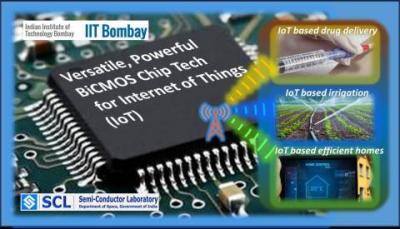
Internet-of- Things (IoT) connects sensors and appliances to computers and the internet to make an intelligent system. Essentially, this networked system can “see” situations instantaneously (through sensors), make “smart decisions” (using the internet), and respond (with tool/appliance) seamlessly. It requires many specialized integrated circuits (ICs) to create this network in different environments of national interest e.g. a home, hospital, factory or paddy field. For example, a sensor IC may measure (e.g. soil moisture or room temperature or blood oxygen level in a patient) and communicate to a controller IC to enable a response (e.g. optimal irrigation or energy-efficient air- conditioning or timely drug delivery respectively). The sensors are normally “analog” as it reports a specific value of moisture/temperature /oxygen within a range – while this is converted into a simplified “digital” information in a computer for decision-making. Thus, such new age applications require versatile ICs capable of processing both analog and digital information (i.e. mixed signal). Bi-CMOS (short for Bipolar-CMOS) technology enables mixed signal ICs. It combines two transistor technologies in one chip – the high-speed and high power Bipolar Junction Transistor (BJT), and Low speed and low power Complementary Metal Oxide Semiconductor (CMOS). In simple terms, CMOS is equivalent of miniature on-off switches (i.e. digital) while BJTs are like miniature fan regulator dials (i.e. analog) that smoothly control the fan-speed. The result is a versatile technology platform in terms of integrated digital-analog (i.e. mixed) signal ICs, with optimal performance based on the choice of high speed (BJT) and low power (CMOS), which strongly enables IoT applications.
India’s strategic needs are served by the 180-nanometer CMOS technology at ISRO Semi Conductor Labs (SCL), Chandigarh. A team from IIT Bombay lead by Prof. Udayan Ganguly has been collaborating with SCL to add BJT technology to the existing CMOS manufacturing baseline at SCL to indigenously develop BiCMOS technology. In May 2016, Dr. Piyush Bhatt, kick-started the project by developing process design for nano-fabrication based on existing SCL capabilities and demonstrating the technical feasibility through computer simulations. Next, the equivalent process was implemented in the IC fabrication lab by a team under Mr. H S. Jatana at SCL. In June 2017, the fabricated devices showed first signs of life! The device amplified the input signal 100 times at the output! In fact, it worked so well that this amplification is sufficient for the first version of BiCMOS technology. Prof. Devang Khakhar, Director, IIT Bombay notes, “Such successful joint technology development attests to skill and the readiness of the Indian Agencies to indigenously enhance our capabilities – which is the first step towards market competitiveness in technology.”
India’s electronic consumption could outstrip its oil consumption by 2020 according to National Electronics Policy 2011. The Government of India is pushing mega-fabs (large-scale chip factories) to support this need. Shri Surinder Singh, Director, SCL has the enviable experience of already running a smaller but high-tech CMOS fab in India. “Mega-fabs are necessary but the ultimate goal is technology autonomy – enabled by indigenous technology development capability. Here, we have leveraged the world-class expertise of IIT Bombay to enable a manufacturable technology development at SCL. This collaborative model works!” remarks Singh. Strategic agencies have always needed to innovate around various international technology restrictions. An Indian semiconductor manufacturing enhanced with the ability for indigenous technology development significantly improves national access to technology that is custom, unique and secure focused on national needs & priorities. Spurred on by the success, the team is working towards higher frequency BiCMOS technology.
This involves further engineering to incorporate new materials into the SCL fab using advanced processes. For example, replacing Silicon atoms with Germanium distorts the crystal and speed up electrons to enable 1000x faster systems. Such high-speed systems are used in high-end communications systems. Prof. Udayan Ganguly’s team works at the bustling Center of Excellence in Nanoelectronics (CEN) at IIT Bombay, which was seeded by the Ministry of Electronics and IT (MeitY) in 2005. Debashis Dutta, Group Coordinator, R&D in Electronics, MeitY, says, “The research success of CEN at IIT Bombay is well known. However, the technology translation stories are coming out. I believe, these are signs of great things to come – which is essentially the realization of a vision of our Ministry for Make in India in ESDM (Electronics Systems Design and Manufacturing)”.
Prof. Udayan Ganguly
