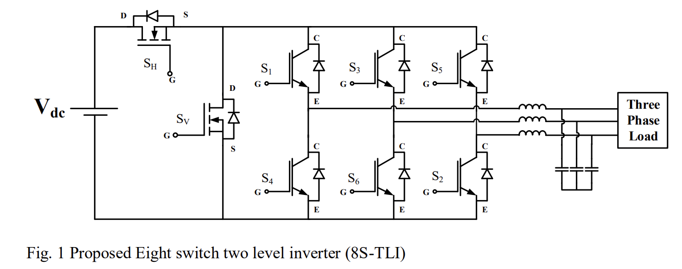
Inverters play a crucial role in modern electrical systems, powering applications from renewable energy integration to industrial drives. Efficiency improvements in these devices lead to smaller equipment sizes, better heat management, and increased profitability. This patent introduces a novel eight-switch two-level hybrid inverter design aimed at enhancing efficiency without compromising cost-effectiveness. By integrating advanced SiC (Silicon Carbide) and Si (Silicon) semiconductor technologies, the inverter achieves Zero Voltage Switching (ZVS) across its main switches. This innovation eliminates the need for traditional passive components like inductors and capacitors, reducing losses significantly. Simulation and experimental tests validate the design, showing substantial efficiency gains especially at higher frequencies, making it suitable for applications prioritizing efficiency and compactness.
Current inverters used in electrical systems face challenges such as inefficient operation at high switching frequencies, leading to increased losses and size requirements. These inefficiencies hinder advancements in reducing equipment size, managing heat effectively, and improving overall profitability. Additionally, integrating advanced semiconductor technologies like SiC and GaN to enhance efficiency often incurs high costs, limiting their widespread adoption. Thus, there is a need for an innovative inverter design that can effectively balance efficiency improvements with economic feasibility, addressing these challenges in modern electrical applications.
- Hybrid Configuration: Integrates both cost-effective Si and high-efficiency SiC devices, striking a balance between performance, efficiency and affordability in inverters.
- Zero Voltage Switching (ZVS): Eliminates the need for traditional passive components like inductors and capacitors, optimizing space vector technique and reducing overall system costs.
- SiC MOSFET Integration: Enables efficient switching operations with reduced losses, enhancing the inverter's reliability and longevity.
- High-Frequency Operation: Supports increased switching frequencies, leading to smaller and more compact inverter designs by minimizing the size of filtering components.
- Improved Efficiency: Demonstrates significant efficiency gains across different load conditions, ensuring optimal energy utilization and operational cost savings.
- Reduces energy consumption and operational costs in diverse electrical applications.
- Promotes sustainable energy practices with enhanced efficiency in inverters.
- Contributes to environmental conservation by minimizing energy wastage.
- Supports reliable power supply for critical infrastructure and services.
- Facilitates integration of renewable energy sources into the grid efficiently.
- Enhances technological advancement in power electronics for broader societal benefits.
Power electronics, Renewable energy sector, Electrical equipment manufacturing
Renewable energy integration, Motor drives, Grid interconnection, Uninterruptible power supplies
Geography of IP
Type of IP
201921041958
452794

