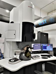
Transmission Electron Microscopy Facility (300 kV)@MEMS

Booking Link
The transmission electron microscope is a 300kV high-resolution microscope with a field emission gun and excellent analytical performance. This facility is used for analysis of elemental composition by energy dispersive spectroscopy, diffraction for crystal structure determination and crystallographic studies.
Make and Model
Thermo Scientific, Themis 300 G3
Available mode for use
Conventional TEM mode
Scanning TEM mode
Spectrum Imaging (EDS)
Tomography
Local Orientation and Stress (A-Star) – to be installed with RIFC support.
Available detectors :
Super-X (EDS), Conventional TEM and STEM
Specifications/Features
Point resolution – 0.2 nm for TEM, 0.12 nm for STEM
Information limit – 0.18 nm
Minimum Brightness – 9.88 x 10⁷ A/m2srV
EDS energy resolution at Mn – 125 eV
Maximum spot drift – 0.45 nm/min
Application
Deformation in metals
Nano science/Nano Technology
Thin Films
Energy Science/Engineering
Chemical composition and quantification (TEM)
Elemental Mapping (STEM)
Tomography
Facility in-charge
Contact Email
Contact no.
022-2159-6765 , +917506110754 (Mr Prakash Ishte)
Location
Room No. 027, Ground Floor, MEMS Department.
Other contact person(s)
- Prakash Ishte
Facility Management Member(s)
(w.e.f. )
Prof. I Samajdar
Prof. Nagamani J. Balila
Prof. Ashutosh Gandhi
Prof. MJNV Prasad
Prof. K G Suresh
Prof. Sushil Mishra
Prof. P J. Guruprasad
Prof. Sankara Sarma V. Tatiparti
